
Universities and Organizations such as the University of California, University of Sheffield, University of Electro-Communications, Okinawa Institute of Science and Technology Graduate University, MIT, University of Toronto, NREL, NIST, NRL … ALL are seeking new discoveries, new methods of application-processes … to achieve the actualization and implementation of “Abundant, Cheap, Renewable Energy”. In this Compilation:
- Singlet Fission – For Increased Efficiencies – 2014-07
- Spray-On Solar Cells – 2014-08
- Pervoskites – A New (LOW COST) Semiconductor Material for Solar Cells – 2014-09
- ‘Dark’ Spin-Triplet Excitons – 2014-10
- Self-Organized Indium Arsenide Quantum Dots for Solar Cells – 2014-09
- A New Breed of “Quantum Dot” Solar Cells – 2014-05
Solar Energy Boost: ‘Singlet Fission’ Could Increase Efficiency by as much as 30%
Jul 08, 2014

A perspective article published last month by University of California, Riverside chemists in the Journal of Physical Chemistry Letters was selected as an Editors Choice—an honor only a handful of research papers receive. The perspective reviews the chemists’ work on “singlet fission,” a process in which a single photon generates a pair of excited states. This 1->2 conversion process, as it is known, has the potential to boost solar cell efficiency by as much as 30 percent.
Applications of the research include more energy-efficient lighting and photodetectors with 200 percent efficiency that can be used for night vision. Biology may use singlet fission to deal with high-energy solar photons without generating excess heat, as a protective mechanism.
Currently, solar cells work by absorbing a photon, which generates an exciton, which subsequently separates into an electron-hole pair. It is these electrons that become solar electricity. The efficiency of these solar cells is limited to about 32 percent, however, by what is called the “Shockley-Queisser Limit.” Future solar cells, also known as “Third Generation” solar cells, will have to surpass this limit while remaining inexpensive, requiring the use of new physical processes. Singlet fission is an example of such a process.
“Our research got its launch about ten years ago when we started thinking about solar energy and what new types of photophysics this might require,” said Christopher Bardeen, a professor of chemistry, whose lab led the research. “Global warming concerns and energy security have made solar energy conversion an important subject from society’s point-of-view. More efficient solar cells would lead to wider use of this clean energy source.”
Research details
When a photon is absorbed, its energy takes the form of an exciton inside the material. Bardeen explained that excitons come in two “flavors,” defined by the electron spins in them. One flavor is singlet, where all spins are paired. The other flavor is triplet, where two electrons are unpaired. In organic semiconductors, these two types of excitons have different energies.
“If a triplet exciton has half the energy of a singlet, then it is possible for one singlet exciton, generated by one photon, to split into two triplet excitons,” Bardeen said. “Thus, you could have a 200 percent yield of excitons—and hopefully, electrons—per absorbed photon.”
He explained that the Shockley-Queisser Limit involves photon absorption to create an exciton, which is basically a bound electron (- charge) and hole (+ charge) pair. In order to get useful electron flow (photocurrent), these excitons must be dissociated. Ideally, one exciton produces one electron (hole) and thus current to run, say, a light bulb.
“To absorb a photon, the photon energy has to be greater than the bandgap of the semiconductor, so you already miss part of the solar spectrum,” Bardeen said. “But if you absorb a photon with energy higher than the bandgap, it has too much energy, and that excess energy is usually wasted as heat. The trick is to take that high energy exciton and split the energy into two excitons, rather than dissipating it as heat.”
Bardeen explained that the singlet exciton spontaneously splits into the two triplets, through a mechanism that is still under active investigation.
“The exact mechanism is unknown, but it does happen quickly—at the sub-nanosecond timescale—and with high efficiency,” he said. “Our work has shown that it is very sensitive to the alignment and position of the two molecules—at least two are required, since we have two excitons—involved in singlet fission. Recent work at MIT has already demonstrated an organic photovoltaic cell with more than 100 percent external quantum efficiency based on this effect. It may be possible to integrate this effect with inorganic semiconductors and use it to raise their efficiencies.”
Next, Bardeen’s lab will look for new materials that exhibit singlet fission, figure out how to take the triplet excitons and turn them into photocurrent efficiently, and look at how the spin properties of the electrons affect the exciton dynamics.
 Scientists develop pioneering new spray-on solar cells

Aug 01, 2014
A team of scientists at the University of Sheffield are the first to fabricate perovskite solar cells using a spray-painting process – a discovery that could help cut the cost of solar electricity.
Published on Mar 4, 2013
A robot spray-coating glass with the polymer to create a solar cell. The technology could one day be used on glass in buildings and cars. For more information about our solar cell research visit http://www.sheffield.ac.uk/physics
Experts from the University’s Department of Physics and Astronomy and Department of Chemical and Biological Engineering have previously used the spray-painting method to produce solar cells using organic semiconductors – but using perovskite is a major step forward.
Efficient organometal halide perovskite based photovoltaics were first demonstrated in 2012. They are now a very promising new material for solar cells as they combine high efficiency with low materials costs.
The spray-painting process wastes very little of the perovskite material and can be scaled to high volume manufacturing – similar to applying paint to cars and graphic printing.
Lead researcher Professor David Lidzey said: “There is a lot of excitement around perovskite based photovoltaics.
“Remarkably, this class of material offers the potential to combine the high performance of mature solar cell technologies with the low embedded energy costs of production of organic photovoltaics.”
While most solar cells are manufactured using energy intensive materials like silicon, perovskites, by comparison, requires much less energy to make. By spray-painting the perovskite layer in air the team hope the overall energy used to make a solar cell can be reduced further.
Professor Lidzey said: “The best certified efficiencies from organic solar cells are around 10 per cent. “Perovskite cells now have efficiencies of up to 19 per cent. This is not so far behind that of silicon at 25 per cent – the material that dominates the world-wide solar market.”
He added: “The perovskite devices we have created still use similar structures to organic cells. What we have done is replace the key light absorbing layer – the organic layer – with a spray-painted perovskite. “Using a perovskite absorber instead of an organic absorber gives a significant boost in terms of efficiency.”
The Sheffield team found that by spray-painting the perovskite they could make prototype solar cells with efficiency of up to 11 per cent.
Professor Lidzey said: “This study advances existing work where the perovskite layer has been deposited from solution using laboratory scale techniques. It’s a significant step towards efficient, low-cost solar cell devices made using high volume roll-to-roll processing methods.”
Solar power is becoming an increasingly important component of the world-wide renewables energy market and continues to grow at a remarkable rate despite the difficult economic environment.
Professor Lidzey said: “I believe that new thin-film photovoltaic technologies are going to have an important role to play in driving the uptake of solar-energy, and that perovskite based cells are emerging as likely thin-film candidates. “
 New “Dirt Cheap” Solar Cells

Sep 24, 2014
One of the most common complaints about solar power is solar panels are still too expensive to be worth the investment. Many researchers have responded by making solar cells, the tile-like components of solar panels that absorb and transfer energy, more efficient and longer lasting. But even the longest living solar cells that most effectively convert sunlight to energy will not become common if they are prohibitively expensive.
Therefore, Professor Yabing Qi, the head of the Energy Materials and Surface Sciences Unit at the Okinawa Institute of Science and Technology Graduate University, has a different idea: make solar cells using a type of semiconductor called perovskite materials, which are, in Qi’s words, “dirt cheap.” If solar cells are cheap enough, Qi reasons that people will want to use them for the immediate payback in energy savings.
Now Professor Qi and members of his research unit have developed a new method for making perovskite solar cells worthy of attention, and The Royal Society of Chemistry published their findings September 5, 2014 in their journal, Energy & Environmental Science.
Qi’s new method uses what he calls hybrid deposition to create perovskite solar cells, made from a mixture of inexpensive organic and inorganic raw materials. In addition, his solar cell is about a thousand times thinner than a silicon solar cell, and therefore uses far less material.
Qi estimates that for the same price, he could either buy raw materials to build 1000 square meters of his solar cell, or he could buy about 20 wafers of crystallized silicon, to build 0.16 square meters of traditional solar panels. “Silicon is not rare,” Qi explains, “but processing silicon requires expensive equipment and sophisticated steps demanding high temperature, vacuum, or high pressure, and that makes crystallized silicon very expensive.”
In contrast, the hybrid deposition process uses less energy to produce a solar cell at a far lower temperature. In fact, Qi envisions manufacturing the new solar cells using a low-cost printing process. The process would deposit the materials onto thin sheets of PET plastic very quickly to make large quantities of cheap solar cells. Qi does not yet know the limits of his hybrid cells, but optimists in his field hope that they could reach 20% efficiency. This means that that the solar cells will convert 20% of the energy they absorb from the sun into usable energy, which is comparable to the best silicon solar panels on the market.
The extremely thin perovskite cell that Qi and his lab designed measures merely 135 nanometers and reaches an efficiency of 9.9%. Because these films are semitransparent, Qi hopes to use them on windows, as a sort of lightweight set of blinds. “It will be a window and at the same time it will be a solar cell,” he says. “Some of the light could go through and the rest will be absorbed. Then, a certain percentage of the absorbed light will be converted to electricity.”
If solar cells are cheap enough, consumers will reap almost immediate benefits even if the solar cells are not the most efficient, because their savings on air conditioning and electricity will offset the expense. “If it’s so cheap that it is like wallpaper, then you might as well use it,” said Qi. “It’s like a free gift. It’s an investment with a lot of payback.”
 Hybrid Materials could Smash the Solar Efficiency Ceiling

October 9, 2014
A new method for transferring energy from organic to inorganic semiconductors could boost the efficiency of widely used inorganic solar cells.
Researchers have developed a new method for harvesting the energy carried by particles known as ‘dark’ spin-triplet excitons with close to 100% efficiency, clearing the way for hybrid solar cells which could far surpass current efficiency limits.
The team, from the University of Cambridge, have successfully harvested the energy of triplet excitons, an excited electron state whose energy in harvested in solar cells, and transferred it from organic to inorganic semiconductors. To date, this type of energy transfer had only been shown for spin-singlet excitons. The results are published in the journal Nature Materials.
In the natural world, excitons are a key part of photosynthesis: light photons are absorbed by pigments and generate excitons, which then carry the associated energy throughout the plant. The same process is at work in a solar cell.
In conventional semiconductors such as silicon, when one photon is absorbed it leads to the formation of one free electron that can be extracted as current. However, in pentacene, a type of organic semiconductor, the absorption of a photon leads to the formation of two electrons. But these electrons are not free and they are difficult to pin down, as they are bound up within ‘dark’ triplet exciton states.
Excitons come in two ‘flavours’: spin-singlet and spin-triplet. Spin-singlet excitons are ‘bright’ and their energy is relatively straightforward to harvest in solar cells. Triplet-spin excitons, in contrast, are ‘dark’, and the way in which the electrons spin makes it difficult to harvest the energy they carry.
“The key to making a better solar cell is to be able to extract the electrons from these dark triplet excitons,” said Maxim Tabachnyk of the University’s Cavendish Laboratory, the paper’s lead author. “If we can combine materials like pentacene with conventional semiconductors like silicon, it would allow us to break through the fundamental ceiling on the efficiency of solar cells.”
Using state-of-art femtosecond laser spectroscopy techniques, the team discovered that triplet excitons could be transferred directly into inorganic semiconductors, with a transfer efficiency of more than 95%. Once transferred to the inorganic material, the electrons from the triplets can be easily extracted.
“Combining the advantages of organic semiconductors, which are low cost and easily processable, with highly efficient inorganic semiconductors, could enable us to further push the efficiency of inorganic solar cells, like those made of silicon,” said Dr Akshay Rao, who lead the team behind the work.
The team is now investigating how the discovered energy transfer of spin-triplet excitons can be extended to other organic/inorganic systems and are developing a cheap organic coating that could be used to boost the power conversion efficiency of silicon solar cells.
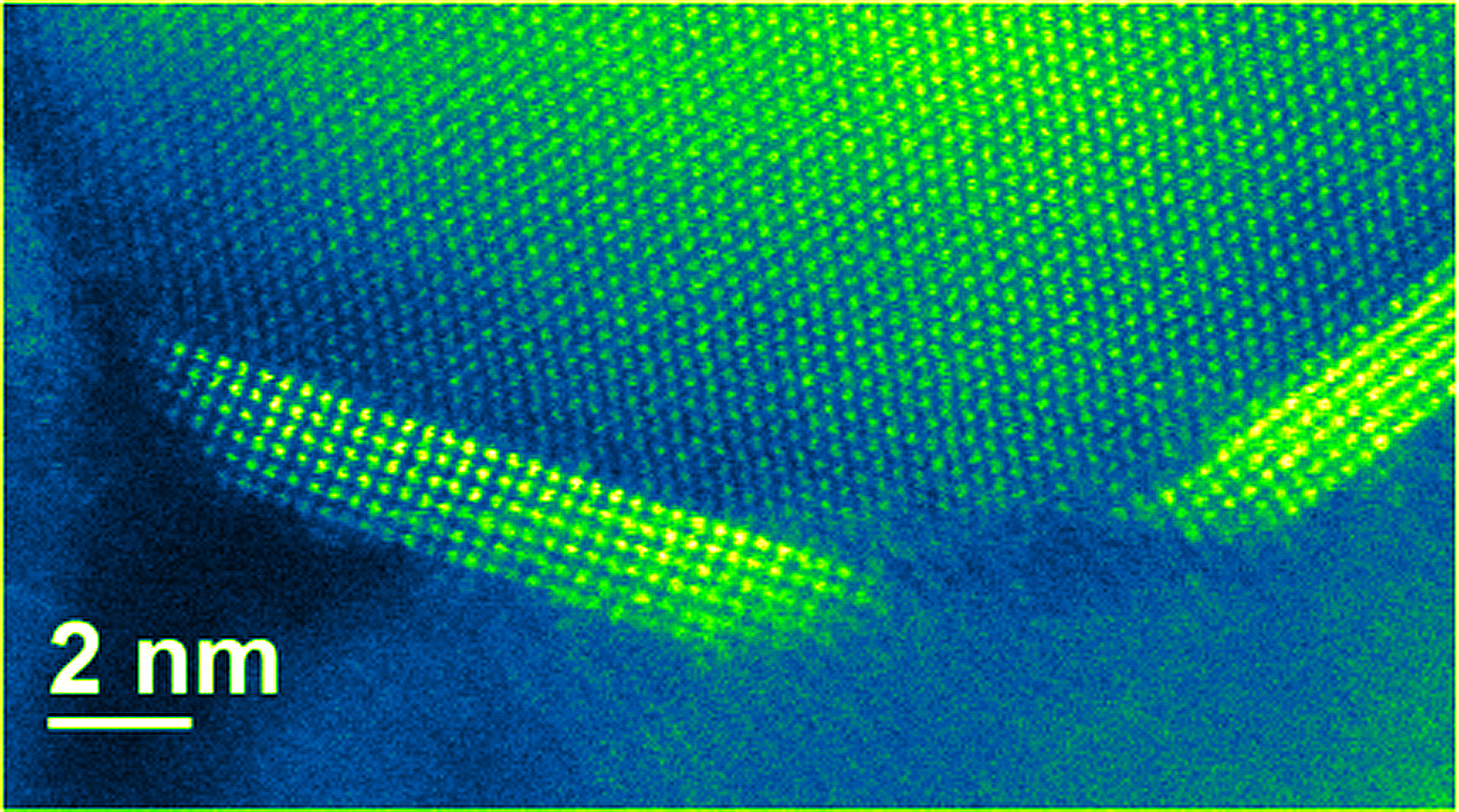
 Self-Organized Indium Arsenide Quantum Dots for Solar Cells

Sep 25, 2014
Kouichi Yamaguchi is internationally recognized for his pioneering research on the fabrication and applications of ‘semiconducting quantum dots’ (QDs). “We exploit the ‘self-organization’ of semiconducting nanocrystals by the ‘Stranski-Krasnov (SK) mode of crystal growth for producing ordered, highly dense, and highly uniform quantum dots,” explains Yamaguchi. “Our ‘bottom-up’ approach yields much better results than the conventional photolithographic or ‘top-down’ methods widely used for the fabrication of nano-structures.”
Notably, electrons in quantum dot structures are confined inside nanometer sized three dimension boxes. Novel applications of ‘quantum dots‘—including lasers, biological markers, qubits for quantum computing, and photovoltaic devices—arise from the unique opto-electronic properties of the QDs when irradiated with light or under external electromagnetic fields.
“Our main interest in QDs is for the fabrication of high efficiency solar cells,” says Yamaguchi. “Step by step we have pushed the limits of ‘self-organization’ based growth of QDs and succeeded in producing highly ordered, ultra-high densities of QDs.”
The realization of an unprecedented QDs density of 5 x 1011 cm-2 in 2011 was one of the major milestones in the development of ‘self-organization‘ based semiconducting QDs for solar cells by Yamaguchi and his colleagues at the University of Electro-Communications (UEC). “This density was one of the critical advances for achieving high efficiency quantum dot based photo-voltaic devices,” says Yamaguchi.
Specifically, Yamaguchi and his group used molecular beam epitaxy (MBE) to grow a layer of InAs QDs with a density of 5 x 1011 cm-2 on GaAsSb/GaAs (100) substrates. Importantly, the breakthrough that yielded this high density of highly ordered QDs was the discovery that InAs growth at a relatively low substrate temperature of 470 degrees Celsius on Sb-irradiated GaAs layers suppressed coalescence or ‘ripening’ of InAs QDs that was observed at higher temperatures. Thus the combination of the Sb surfactant effect and lower growth temperature yielded InAs QDs with an average height of 2.02.5 nm.

The potential for photovoltaic device applications was examined by sandwiching a single layer of InAs QDs in a pin-GaAs cell structure. The resulting external quantum efficiency of these solar cell structures in the 900 to 1150 nm wavelength range was higher than devices with the QD layer.
“Theoretical studies suggest QDs solar cells could yield conversion efficiencies over 50%,” explains Yamaguchi. “This is a very challenging target but we hope that our innovative approach will be an effective means of producing such QD based high performance solar cells. We have recently achieved InAs QDs with a density of 1 x 1012 cm-2.”

Variation of power conversion efficiency with quantum dot density (calculated results). Enlarge
 Quantum Dot Photovoltaics: A New Breed of Solar Cells: Setting New Records for Efficiency

May 28, 2014
Solar-cell technology has advanced rapidly, as hundreds of groups around the world pursue more than two dozen approaches using different materials, technologies, and approaches to improve efficiency and reduce costs.
Now a team at MIT has set a new record for the most efficient quantum-dot cells—a type of solar cell that is seen as especially promising because of its inherently low cost, versatility, and light weight.
While the overall efficiency of this cell is still low compared to other types—about 9 percent of the energy of sunlight is converted to electricity—the rate of improvement of this technology is one of the most rapid seen for a solar technology. The development is described in a paper, published in the journal Nature Materials, by MIT professors Moungi Bawendi and Vladimir Bulović and graduate students Chia-Hao Chuang and Patrick Brown.
The new process is an extension of work by Bawendi, the Lester Wolfe Professor of Chemistry, to produce quantum dots with precisely controllable characteristics—and as uniform thin coatings that can be applied to other materials. These minuscule particles are very effective at turning light into electricity, and vice versa. Since the first progress toward the use of quantum dots to make solar cells, Bawendi says, “The community, in the last few years, has started to understand better how these cells operate, and what the limitations are.”
The new work represents a significant leap in overcoming those limitations, increasing the current flow in the cells and thus boosting their overall efficiency in converting sunlight into electricity.
Many approaches to creating low-cost, large-area flexible and lightweight solar cells suffer from serious limitations—such as short operating lifetimes when exposed to air, or the need for high temperatures and vacuum chambers during production.
By contrast, the new process does not require an inert atmosphere or high temperatures to grow the active device layers, and the resulting cells show no degradation after more than five months of storage in air.
Bulović, the Fariborz Maseeh Professor of Emerging Technology and associate dean for innovation in MIT’s School of Engineering, explains that thin coatings of quantum dots “allow them to do what they do as individuals—to absorb light very well—but also work as a group, to transport charges.” This allows those charges to be collected at the edge of the film, where they can be harnessed to provide an electric current.
The new work brings together developments from several fields to push the technology to unprecedented efficiency for a quantum-dot based system: The paper’s four co-authors come from MIT’s departments of physics, chemistry, materials science and engineering, and electrical engineering and computer science. The solar cell produced by the team has now been added to the National Renewable Energy Laboratories’ listing of record-high efficiencies for each kind of solar-cell technology.
The overall efficiency of the cell is still lower than for most other types of solar cells. But Bulović points out, “Silicon had six decades to get where it is today, and even silicon hasn’t reached the theoretical limit yet. You can’t hope to have an entirely new technology beat an incumbent in just four years of development.” And the new technology has important advantages, notably a manufacturing process that is far less energy-intensive than other types.
Chuang adds, “Every part of the cell, except the electrodes for now, can be deposited at room temperature, in air, out of solution. It’s really unprecedented.”
The system is so new that it also has potential as a tool for basic research. “There’s a lot to learn about why it is so stable. There’s a lot more to be done, to use it as a testbed for physics, to see why the results are sometimes better than we expect,” Bulović says.
A companion paper, written by three members of the same team along with MIT’s Jeffrey Grossman, the Carl Richard Soderberg Associate Professor of Power Engineering, and three others, appears this month in the journal ACS Nano, explaining in greater detail the science behind the strategy employed to reach this efficiency breakthrough.
The new work represents a turnaround for Bawendi, who had spent much of his career working with quantum dots. “I was somewhat of a skeptic four years ago,” he says. But his team’s research since then has clearly demonstrated quantum dots‘ potential in solar cells, he adds.
Arthur Nozik, a research professor in chemistry at the University of Colorado who was not involved in this research, says, “This result represents a significant advance for the applications of quantum-dot films and the technology of low-temperature, solution-processed, quantum-dot photovoltaic cells. … There is still a long way to go before quantum-dot solar cells are commercially viable, but this latest development is a nice step toward this ultimate goal.”


You must be logged in to post a comment.