Quantum Dots leader completes deal to manufacture NextGen Cadmium Free QD’s in Asia


A leading US quantum dot and nanomaterials manufacturer has announced a licensing and manufacturing deal in Assam, India.

The company, Quantum Materials Corp (QMC), has a range of products which can be used to make anything from superior Ultra High Definition television displays to ultra-thin solar cells and more efficient batteries.

The agreement will not only lead to significant job opportunities in the locality of Assam, but is also a major step in deploying QMC’s extraordinary technologies in the region.

There is the opportunity to adopt next-generation solar photovoltaic technology in the area, after the implementation of recent tariffs on imported photovoltaics into India.

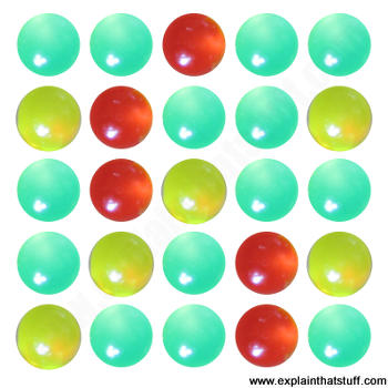
QMC’s cadmium-free quantum dots offer a less hazardous and eco-friendlier alternative for producers and consumers, providing them with the color benefit without the risks of toxicity or liability.

The incorporation of cadmium in quantum dots has restricted their adoption, keeping manufacturers from leveraging the benefits of the technology. Restriction of Hazardous Substances regulations currently state that 1,000 parts per million (ppm) cadmium can be used, however this exception will soon expire and only 100 ppm of cadmium will be acceptable. In 2015, the European Parliament banned the continued use of cadmium in display and lighting devices.

img_0866Read More: What are quantum dots? The Science and Applications

Furthermore, controls and regulations are growing in Asia, with China implementing new laws of its own.

QMC signed the License and Development Agreement with Amtronics CC to allow for the establishment of large scale, low cost quantum dot production for the development and future commercial manufacture of: ultra-high definition display panels, solid state lighting LEDs and quantum dot driven thin-film solar cells.

The Agreement provides Amtronics CC with the right to manufacture quantum dots and thin-film quantum dot solar cells for commercial supply in India, as well as the right to use the QDXTM trademark and technical data to support its marketing initiatives. Under the terms of the Agreement, QMC receives an immediate upfront license fee of US$1,000,000 in addition to technology development funding, scheduled milestone payments and royalties on all quantum dots/solar cells produced.

The 12,000 square feet nanotech-focused facility is being established as the anchor project within the recently announced Electronics Manufacturing Cluster in the Guwahati Tech City.

“We are extremely pleased to partner with Amtronics CC and Amtron as they establish the necessary infrastructure to support large scale thin-film, quantum dot based solar cell production in Assam India using QMC patented technologies” explained Stephen B. Squires, President and CEO of Quantum Materials Corp.

“India’s recent implementation of tariffs applied to imported solar photovoltaics creates an ideal opportunity to establish QMC’s next generation thin-film photovoltaics for broad adoption in the region. I am highly confident that our technologies will help India fulfill its goal to deploy low cost renewables as a significant step toward energy independence”

Dr. George Anthony Balchin, Managing Director of Amtronics CC added, “We are pleased to be involved and provide the initial US $20,000,000 in funding for this enterprise and are anxious to see these extraordinary technologies deployed in a region that will benefit from both the end product as well as the significant potential for job creation.

The initial capital infusion will be used to build out the facility, purchase all the production and process equipment, including the micro reactors, train the staff and provide the initial working capital. It is very rare and rewarding to be involved with a project that is the culmination of a group of like-minded individuals striving for a common goal that has so much potential to enhance the lives of so many.”

Commenting further QMC CEO Squires stated: “As India represents one of the largest renewable energy and consumer electronics markets in the world, our partnership with Amtronics CC is an important step in expanding the value of the QMC franchise globally. This partnership will allow us to address global challenges such as rising energy costs, energy security, increasing power consumption and environmental quality on a more rapid basis.”

ASU and Stanford Researchers Achieve Record Breaking Efficiency with Tandem (Perovskite + Silicon) Solar Cell


ecee-perovskite-silicon-tandem-cell-pz-0035-w-1280x640Above: A perovskite/silicon tandem solar cell, created by research teams from Arizona State University and Stanford University, capable of record-breaking sunlight-to-electricity conversion efficiency. Photographer: Pete Zrioka/ASU

Some pairs are better together than their individual counterparts — peanut butter and chocolate, warm weather and ice cream, and now, in the realm of photovoltaic technology, silicon and perovskite.

As existing solar energy technologies near their theoretical efficiency limits, researchers are exploring new methods to improve performance — such as stacking two photovoltaic materials in a tandem cell. Collaboration between researchers at Arizona State University and Stanford University has birthed such a cell with record-breaking conversion efficiency — effectively finding the peanut butter to silicon’s chocolate.

ecee-holman-lab-jh-1123w

The results of their work, published February 17 in Nature Energy, outline the use of perovskite and silicon to create a tandem solar cell capable of converting sunlight to energy with an efficiency of 23.6 percent, just shy of the all-time silicon efficiency record.

“The best silicon solar cell alone has achieved 26.3 percent efficiency,” says Zachary Holman, an assistant professor of electrical engineering at the Ira A. Fulton Schools of Engineering. “Now we’re gunning for 30 percent with these tandem cells, and I think we could be there within two years.”

Assistant Professor Zachary Holman, holds one of the many solar cells his research group has created. Photographer: Jessica Hochreiter/ASU

Silicon solar cells are the backbone of a $30 billion a year industry, and this breakthrough shows that there’s room for significant improvement within such devices by finding partner materials to boost efficiency.

The high-performance tandem cell’s layers are each specially tuned to capture different wavelengths of light. The top layer, composed of a perovskite compound, was designed to excel at absorbing visible light. The cell’s silicon base is tuned to capture infrared light.

Perovskite, a cheap, easily manufacturable photovoltaic material, has emerged as a challenger to silicon’s dominance in the solar market. Since its introduction to solar technology in 2009, the efficiency of perovskite solar cells has increased from 3.8 percent to 22.1 percent in early 2016, according to the National Renewable Energy Laboratory.

The perovskite used in the tandem cell came courtesy of Stanford researchers Professor Michael McGehee and doctoral student Kevin Bush, who fabricated the compound and tested the materials.

The research team at ASU provided the silicon base and modeling to determine other material candidates for use in the tandem cell’s supporting layers.

OVERCOMING CHALLENGES WITH PEROVSKITES

 Zhengshan (Jason) Yu, an electrical engineering doctoral student at ASU, holds up a tiny black solar cell which is flanked by two conductors. The small cell has yielded big improvements, resulting in a record-breaking 23.6 percent efficiency rate.

Though low-cost and highly efficient, perovskites have been limited by poor stability, degrading at a much faster rate than silicon in hot and humid environments. Additionally, perovskite solar cells have suffered from parasitic absorption, in which light is absorbed by supporting layers in the cell that don’t generate electricity.

“We have improved the stability of the perovskite solar cells in two ways,” says McGehee, a materials science and engineering professor at Stanford’s School of Engineering. “First, we replaced an organic cation with cesium. Second, we protected the perovskite with an impermeable indium tin oxide layer that also functions as an electrode.”

Though McGehee’s compound achieves record stability, perovskites remain delicate materials, making it difficult to employ in tandem solar technology.

“In many solar cells, we put a layer on top that is both transparent and conductive,” says Holman, a faculty member in the School of Electrical, Computer and Energy Engineering. “It’s transparent so light can go through and conductive so we can take electrical charges off it.”

This top conductive layer is applied using a process called sputtering deposition, which historically has led to damaged perovskite cells. However, McGehee was able to apply a tin oxide layer with help from chemical engineering Professor Stacey Bent and doctoral student Axel Palmstrom of Stanford. The pair developed a thin layer that protects the delicate perovskite from the deposition of the final conductive layer without contributing to parasitic absorption, further boosting the cell’s efficiency.

The deposition of the final conductive layer wasn’t the only engineering challenge posed by integrating perovskites and silicon.

“It was difficult to apply the perovskite itself without compromising the performance of the silicon cell,” says Zhengshan (Jason) Yu, an electrical engineering doctoral student at ASU.

Silicon wafers are placed in a potassium hydroxide solution during fabrication, which creates a rough, jagged surface. This texture, ideal for trapping light and generating more energy, works well for silicon, but perovskite prefers a smooth — and unfortunately reflective — surface for deposition.

Additionally, the perovskite layer of the tandem cell is less than a micron thick, opposed to the 250-micron thick silicon layer. This means when the thin perovskite layer was deposited, it was applied unevenly, pooling in the rough silicon’s low points and failing to adhere to its peaks.

Yu developed a method to create a planar surface only on the front of the silicon solar cell using a removable, protective layer. This resulted in a smooth surface on one side of the cell, ideal for applying the perovskite, while leaving the backside rough, to trap the weakly-absorbed near-infrared light in the silicon.

“With the incorporation of a silicon nanoparticle rear reflector, this infrared-tuned silicon cell becomes an excellent bottom cell for tandems,” says Yu.

BUILDING ON PREVIOUS SUCCESSES

The success of the tandem cell is built on existing achievements from both teams of researchers. In October 2016, McGehee and post-doctoral scholar Tomas Leijtens fabricated an all-perovskite cell capable of 20.3 percent efficiency. The high-performance cell was achieved in part by creating a perovskite with record stability, marking McGehee’s group as one of the first teams to devote research efforts to fabricating stable perovskite compounds.

Likewise, Holman has considerable experience working with silicon and tandem cells.

“We’ve tried to position our research group as the go-to group in the U.S. for silicon bottom cells for tandems,” says Holman, who’s been pursuing additional avenues to create high-efficiency tandem solar cells.

In fact, Holman and Yu published a comment in Nature Energy in September 2016 outlining the projected efficiencies of different cell combinations in tandems.

“People often ask, ‘given the fundamental laws of physics, what’s the best you can do?’” says Holman. “We’ve asked and answered a different, more useful question: Given two existing materials, if you could put them together, ideally, what would you get?”’

The publication is a sensible guide to designing a tandem solar cell, specifically with silicon as the bottom solar cell, according to Holman.

It calculates what the maximum efficiency would be if you could pair two existing solar cells in a tandem without any performance loss. The guide has proven useful in directing research efforts to pursue the best partner materials for silicon.

“We have eight projects with different universities and organizations, looking at different types of top cells that go on top of silicon,” says Holman. “So far out of all our projects, our perovskite/silicon tandem cell with Stanford is the leader.”

NREL: Nanoscale confinement leads to new all-inorganic perovskite with exceptional solar cell properties – Using Quantum Dots to Create Increased Solar Cell Efficiency: Colorado School of Mines


confinement-for-qdots-100816-nanoscaleconAshley Marshall, Erin Sanehira and Joey Luther with solutions of all-inorganic perovskite quantum dots, showing intense photoluminescence when illuminated with UV light. Credit: National Renewable Energy Laboratory

Scientists with the Energy Department’s National Renewable Energy Laboratory (NREL) for the first time discovered how to make perovskite solar cells out of quantum dots and used the new material to convert sunlight to electricity with 10.77 percent efficiency.

The research, Quantum dot-induced phase stabilization of a-CsPbI3 perovskite for high-efficiency photovoltaics, appears in the journal Science. The authors are Abhishek Swarnkar, Ashley Marshall, Erin Sanehira, Boris Chernomordik, David Moore, Jeffrey Christians, and Joseph Luther from NREL. Tamoghna Chakrabarti from the Colorado School of Mines also is a co-author.co-school-of-mines-222925_original

In addition to developing quantum dot , the researchers discovered a method to stabilize a crystal structure in an all-inorganic perovskite material at room temperature that was previously only favorable at high temperatures. The crystal phase of the inorganic material is more stable in .

Most research into perovskites has centered on a hybrid organic-inorganic structure. Since research into perovskites for photovoltaics began in 2009, their efficiency of converting sunlight into electricity has climbed steadily and now shows greater than 22 percent power conversion efficiency. However, the organic component hasn’t been durable enough for the long-term use of perovskites as a solar cell.

NREL scientists turned to quantum dots-which are essentially nanocrystals-of cesium lead iodide (CsPbI3) to remove the unstable and open the door to high-efficiency quantum dot optoelectronics that can be used in LED lights and photovoltaics. NREL 20140609_buildings_26954_hp

The nanocrystals of CsPbI3 were synthesized through the addition of a Cs-oleate solution to a flask containing PbI2 precursor. The NREL researchers purified the nanocrystals using methyl acetate as an anti-solvent that removed excess unreacted precursors. This step turned out to be critical to increasing their stability.

Contrary to the bulk version of CsPbI3, the nanocrystals were found to be stable not only at temperatures exceeding 600 degrees Fahrenheit but also at room temperatures and at hundreds of degrees below zero. The bulk version of this material is unstable at , where photovoltaics normally operate and convert very quickly to an undesired crystal structure.

NREL scientists were able to transform the nanocrystals into a thin film by repeatedly dipping them into a methyl acetate solution, yielding a thickness between 100 and 400 nanometers. Used in a solar cell, the CsPbI3 nanocrystal film proved efficient at converting 10.77 percent of sunlight into electricity at an extraordinary high open circuit voltage. The efficiency is similar to record quantum dot solar cells of other materials and surpasses other reported all-inorganic perovskite solar cells.

Explore further: Rubidium pushes perovskite solar cells to 21.6 percent efficiency

More information: A. Swarnkar et al. Quantum dot-induced phase stabilization of -CsPbI3 perovskite for high-efficiency photovoltaics, Science (2016). DOI: 10.1126/science.aag2700


Elon Musk: Solar Panels Will Be Your New Roof … And His Vision for a ‘Solar Future’


Solar Cells 041115 organicsemic

Elon Musk has confirmed the next step in the evolution of sustainable energy: Rather than adding solar panels to an existing roof, the panels will BE the roof. What seems like an obvious progression for this technology is actually a unique move in the market.

The news came out of SolarCity‘s conference call yesterday, covering its second quarter financial results, as reported by Electrek. Following SolarCity CEO Lyndon Rive’s reference to 2 new products expected in 2017, Musk jumped in to add “It’s a solar roof, as opposed to modules on a roof… think this is really a fundamental part of achieving differentiated product strategy, where you have a beautiful roof. It’s not a thing on the roof. It is the roof.”

Rive added that this will allow solar city to access a new market, citing that 5 million new roofs are installed each year in the US alone. Additionally the average homeowner is unlikely to install solar panels on a roof that may need to be replaced in the near future, so a solar roof would be the best option.

SolarCity’s existing ‘retro-fit’ panels will not be axed, confirmed Musk, who believes the new business plan will work alongside SolarCity’s existing products. This doesn’t appear to impact Musk’s proposed plan, which was announced following Tesla’s acquisition of SolarCity

Elon Musk’s Turnkey Vision For Energy Independence

In hishis authentic Elon Musk-ian way, the Tesla cofounder and CEO unveiled the roadmap for future of the electic motor company.

Yesterday, Telsa’s blog posted Elon Musk’s Master Plan Part Deux, the highly anticipated sequel to 2006’s master pan. In Musk’s attempt to make sense of Tesla’s recent moves, he explained the decision to acquire SolarCity and the vision to create a (more) sustainable world.

“The point of all this was, and remains, accelerating the advent of sustainable energy, so that we can imagine far into the future and life is still good. That’s what “sustainable” means. It’s not some silly, hippy thing — it matters for everyone.”said Musk in the statement released July 20, “We can’t do this well if Tesla and SolarCity are different companies, which is why we need to combine and break down the barriers inherent to being separate companies.”

Tesla’s absorption of SolarCity is essential to “create a smoothly integrated and beautiful solar-roof-with-battery product that just works.” At this point it is unclear if this relates exclusively to Tesla’s vehicles, or will also apply the Powerwall, Tesla’s built-for-the-home battery.

Regardless, the future of sustainability (as Musk sees it), is do or die: “By definition, we must at some point achieve a sustainable energy economy or we will run out of fossil fuels to burn and civilization will collapse.”

Elon Musk Reveals Tesla Master Plan that Includes Solar Roofs, 10X Safer Self-Driving, and Car-Sharing

Read more about Musk’s Master Plan here.

Non-toxic and cheap thin-film solar cells for ‘zero-energy’ buildings


Non Toxic Solar Cells 042816 160428103023_1_540x360Dr Xiaojing Hao of UNSW’s Australian Centre for Advanced Photovoltaics holding the new CZTS solar cells.
Credit: Quentin Jones/UNSW

World’s highest efficiency rating achieved for CZTS thin-film solar cells

‘Zero-energy’ buildings — which generate as much power as they consume — are now much closer after a team at Australia’s University of New South Wales achieved the world’s highest efficiency using flexible solar cells that are non-toxic and cheap to make.

Until now, the promise of ‘zero-energy’ buildings been held back by two hurdles: the cost of the thin-film solar cells (used in façades, roofs and windows), and the fact they’re made from scarce, and highly toxic, materials.

That’s about to change: the UNSW team, led by Dr Xiaojing Hao of the Australian Centre for Advanced Photovoltaics at the UNSW School of Photovoltaic and Renewable Energy Engineering, have achieved the world’s highest efficiency rating for a full-sized thin-film solar cell using a competing thin-film technology, known as CZTS.

NREL, the USA’s National Renewable Energy Laboratory, confirmed this world leading 7.6% efficiency in a 1cm2 area CZTS cell this month.

Unlike its thin-film competitors, CZTS cells are made from abundant materials: copper, zinc, tin and sulphur.

And CZTS has none of the toxicity problems of its two thin-film rivals, known as CdTe (cadmium-telluride) and CIGS (copper-indium-gallium-selenide). Cadmium and selenium are toxic at even tiny doses, while tellurium and indium are extremely rare.

“This is the first step on CZTS’s road to beyond 20% efficiency, and marks a milestone in its journey from the lab to commercial product,” said Hao, named one of UNSW’s 20 rising stars last year. “There is still a lot of work needed to catch up with CdTe and CIGS, in both efficiency and cell size, but we are well on the way.”

“In addition to its elements being more commonplace and environmentally benign, we’re interested in these higher bandgap CZTS cells for two reasons,” said Professor Martin Green, a mentor of Dr Hao and a global pioneer of photovoltaic research stretching back 40 years.

“They can be deposited directly onto materials as thin layers that are 50 times thinner than a human hair, so there’s no need to manufacture silicon ‘wafer’ cells and interconnect them separately,” he added. “They also respond better than silicon to blue wavelengths of light, and can be stacked as a thin-film on top of silicon cells to ultimately improve the overall performance.”

By being able to deposit CZTS solar cells on various surfaces, Hao’s team believe this puts them firmly on the road to making thin-film photovoltaic cells that can be rigid or flexible, and durable and cheap enough to be widely integrated into buildings to generate electricity from the sunlight that strikes structures such as glazing, façades, roof tiles and windows.

However, because CZTS is cheaper — and easier to bring from lab to commercialisation than other thin-film solar cells, given already available commercialised manufacturing method — applications are likely even sooner. UNSW is collaborating with a number of large companies keen to develop applications well before it reaches 20% efficiency — probably, Hao says, within the next few years.

“I’m quietly confident we can overcome the technical challenges to further boosting the efficiency of CZTS cells, because there are a lot of tricks we’ve learned over the past 30 years in boosting CdTe and CIGS and even silicon cells, but which haven’t been applied to CZTS,” said Hao.

Currently, thin-film photovoltaic cells like CdTe are used mainly in large solar power farms, as the cadmium toxicity makes them unsuitable for residential systems, while CIGS cells is more commonly used in Japan on rooftops.

First Solar, a US$5 billion behemoth that specialises in large-scale photovoltaic systems, relies entirely on CdTe; while CIGS is the preferred technology of China’s Hanergy, the world’s largest thin-film solar power company.

Thin-film technologies such as CdTe and CIGS are also attractive because they are physically flexible, which increases the number of potential applications, such as curved surfaces, roofing membranes, or transparent and translucent structures like windows and skylights.

But their toxicity has made the construction industry — mindful of its history with asbestos — wary of using them. Scarcity of the elements also renders them unattractive, as price spikes are likely as demand rises. Despite this, the global market for so-called Building-Integrated Photovoltaics (BIPV) is already valued at US$1.6 billion.

Hao believes CZTS’s cheapness, benign environmental profile and abundant elements may be the trigger that finally brings architects and builders onboard to using thin-film solar panels more widely in buildings.

Until now, most architects have used conventional solar panels made from crystalline silicon. While these are even cheaper than CZTS cells, they don’t offer the same flexibility for curved surfaces and other awkward geometries needed to easily integrate into building designs.


Story Source:

The above post is reprinted from materials provided byUniversity of New South Wales. The original item was written by Wilson da Silva. Note: Materials may be edited for content and length.

Solar Cell Mystery Solved! Expected to greatly increase efficiency


(Left) The set-up used to grow single crystals of spiro-OMeTAD, based on antisolvent vapor-assisted crystallization. (Right) Single crystal structure of spiro-OMeTAD. Credit: Shi, et al. ©2016 AAAS


For the past 17 years, spiro-OMeTAD, has been keeping a secret. Despite intense research efforts, its performance as the most commonly used hole-transporting material in perovskite and dye-sensitized solar cells has remained stagnant, creating a major bottleneck for improving solar cell efficiency. 

Thinking that the material has given all it has to offer, many researchers have begun investigating alternative materials to replace spiro-OMeTAD in future solar cells.

But in a new study published in Science Advances, Dong Shi et al. have taken a closer look at spiro-OMeTAD and found that it still has a great deal of untapped potential. For the first time, they have grown single crystals of the pure material, and in doing so, they have made the surprising discovery that spiro-OMeTAD’s single-crystal structure has a hole mobility that is three orders of magnitude greater than that of its thin-film form (which is currently used in solar cells).

“This paper reports a major breakthrough for the fields of perovskite and solid-state dye-sensitized solar cells by finally clarifying the potential performance of the material and showing that improving the crystallinity of the hole transport layer is the key strategy for further breakthroughs in device engineering of these solar cells,” Osman Bakr, a professor of engineering at King Abdullah University of Science and Technology (KAUST) in Saudi Arabia and leader of the study, told Phys.org.

The findings suggest that, at least in the short term, the time-consuming process of designing and synthesizing radically new organic hole conductors as replacements to spiro-OMeTAD may not be necessary.

In general, perovskite solar cells and dye-sensitized solar cells are made of three critical layers. Two of these layers—the electron-transporting layer and the light-absorbing layer—are well-understood structurally. However, the mesoscale packing structure of the hole-transporting layer, which is usually spiro-OMeTAD, has so far eluded researchers, and consequently its charge transport mechanisms have remained a mystery.

In the new study, the researchers figured out a way to grow pure single crystals of spiro-OMeTAD by dissolving the spiro-OMeTAD in a carefully chosen solvent. They then placed this vial inside a larger vial containing an antisolvent, in which spiro-OMeTAD does not dissolve as well, and allowed the antisolvent vapor to slowly diffuse into the inner vial.

Eventually the solution in the inner vial becomes supersaturated, so that not all of the spiro-OMeTAD can stay dissolved, causing the spiro-OMeTAD to crystallize. The researchers then performed a variety of measurements on the crystals to investigate their charge transport mechanisms and other properties.

The results are much more encouraging than expected, in many ways running contrary to the conventional wisdom based on the material’s large-scale structure, which suggested that the material had reached its limits.

Although the method used here to grow single crystals cannot be performed at a large scale, the researchers predict that similar methods that use an antisolvent to trigger crystallization could be used to enhance the crystallinity of the thin-layer spiro-OMeTAD, improving its hole mobility in order to make more efficient solar cells.

“These astonishing findings open a new direction for the development of perovskite solar cells and dye-sensitized solar cells by showing the still untapped potential of spiro-OMeTAD,” Bakr said. “They unravel a key mystery that has confounded the photovoltaic community for the last 17 years.”

More information: Dong Shi, et al. “Spiro-OMeTAD single crystals: Remarkably enhanced charge-carrier transport via mesoscale ordering.” Science Advances. DOI: 10.1126/sciadv.1501491

Abstract 

We report the crystal structure and hole-transport mechanism in spiro-OMeTAD [2,2′,7,7′-tetrakis(N,N-di-p-methoxyphenyl-amine)9,9′-spirobifluorene], the dominant hole-transporting material in perovskite and solid-state dye-sensitized solar cells.

Despite spiro-OMeTAD’s paramount role in such devices, its crystal structure was unknown because of highly disordered solution-processed films; the hole-transport pathways remained ill-defined and the charge carrier mobilities were low, posing a major bottleneck for advancing cell efficiencies.

We devised an antisolvent crystallization strategy to grow single crystals of spiro-OMeTAD, which allowed us to experimentally elucidate its molecular packing and transport properties. Electronic structure calculations enabled us to map spiro-OMeTAD’s intermolecular charge-hopping pathways.

Promisingly, single-crystal mobilities were found to exceed their thin-film counterparts by three orders of magnitude. Our findings underscore mesoscale ordering as a key strategy to achieving breakthroughs in hole-transport material engineering of solar cells.


Genesis Nanotechnology, Inc. ~ “Great Things from Small Things”

Follow Us on Facebook Facebook 

http://Facebook.com/genesisnanotech

 Watch Our YouTube Video:

Solar Cells Will be Made Obsolete by 3D rectennas aiming at 40-to-90% efficiency


Rectenna Naval Optical 150928122542_1_540x360A new kind of nanoscale rectenna (half antenna and half rectifier) can convert solar and infrared into electricity, plus be tuned to nearly any other frequency as a detector.

Right now efficiency is only one percent, but professor Baratunde Cola and colleagues at the Georgia Institute of Technology (Georgia Tech, Atlanta) convincingly argue that they can achieve 40 percent broad spectrum efficiency (double that of silicon and more even than multi-junction gallium arsenide) at a one-tenth of the cost of conventional solar cells (and with an upper limit of 90 percent efficiency for single wavelength conversion).

It is well suited for mass production, according to Cola. It works by growing fields of carbon nanotubes vertically, the length of which roughly matches the wavelength of the energy source (one micron for solar), capping the carbon nanotubes with an insulating dielectric (aluminum oxide on the tethered end of the nanotube bundles), then growing a low-work function metal (calcium/aluminum) on the dielectric and voila–a rectenna with a two electron-volt potential that collects sunlight and converts it to direct current (DC).

“Our process uses three simple steps: grow a large array of nanotube bundles vertically; coat one end with dielectric; then deposit another layer of metal,” Cola told EE Times. “In effect we are using one end of the nanotube as a part of a super-fast metal-insulator-metal tunnel diode, making mass production potentially very inexpensive up to 10-times cheaper than crystalline silicon cells.”

For commercialization, billions or even trillions of carbon-nanotube bundles could be grown side-by-side, ramping up the power output into the megaWatt range, after optimization for higher efficiency.

“We still have a lot of work to do to lower contact resistance which will improve the impedance match between the antenna and diode, thus raising efficiency,” Cola told us.”Our proof-of-concept was tuned to the near-infrared. We used infrared-, solar- and green laser-light and got efficiencies of less than one percent, but what was key to our demo was we showed our computer model matched our experimental results, giving us the confidence that we can improve the efficiency up to 40 percent in just a few years.”

For the future, Cola’s group has a three tiered goal–first develop sensor applications that don’t require high efficiencies, second to get the efficiency to 20 percent for harvesting waste heat in the infrared spectrum, then start replacing standard solar cells with 40 percent efficient panels in the visible spectrum. The team is also seeking suitable flexible substrates for applications that require bending.


Schematic of the components making up the optical rectenna–carbon nanotubes capped with a metal-oxide-metal tunneling diode. (Credit: Thomas Bougher)
(Source: Georgia Tech)

Nature Nanotechnology – A carbon nanotube optical rectenna

An optical rectenna—a device that directly converts free-propagating electromagnetic waves at optical frequencies to direct current—was first proposed over 40 years ago, yet this concept has not been demonstrated experimentally due to fabrication challenges at the nanoscale. Realizing an optical rectenna requires that an antenna be coupled to a diode that operates on the order of 1 pHz (switching speed on the order of 1 fs).

Diodes operating at these frequencies are feasible if their capacitance is on the order of a few attofarads but they remain extremely difficult to fabricate and to reliably couple to a nanoscale antenna. Here we demonstrate an optical rectenna by engineering metal–insulator–metal tunnel diodes, with a junction capacitance of ∼2 aF, at the tip of vertically aligned multiwalled carbon nanotubes (∼10 nm in diameter), which act as the antenna. Upon irradiation with visible and infrared light, we measure a d.c. open-circuit voltage and a short-circuit current that appear to be due to a rectification process (we account for a very small but quantifiable contribution from thermal effects). In contrast to recent reports of photodetection based on hot electron decay in a plasmonic nanoscale antenna a coherent optical antenna field appears to be rectified directly in our devices, consistent with rectenna theory. Finally, power rectification is observed under simulated solar illumination, and there is no detectable change in diode performance after numerous current–voltage scans between 5 and 77 °C, indicating a potential for robust operation.


GNT Thumbnail Alt 3 2015-page-001

Genesis Nanotechnology, Inc. ~ “Great Things from Small Things”

Watch Our YouTube Video

Follow Our ‘Top Ten’ Blog: “Great Things from Small Things”

Follow Us on Twitter: @Genesisnanotech

Follow and ‘Like’ Us on Facebook

Connect with Our Website

‘Join the Conversation’ at Our LinkedIn ‘Nano Network’ Group

Catching more of the sun with Quantum Dots and Organic Molecules 


Published online Mar 20, 2016

Combining quantum dots and organic molecules can enable solar cells to capture more of the sun’s light.

Organic molecules aid charge transfer from large lead sulfide quantum dots for improved solar-cell performance. Light from the sun is our most abundant source of renewable energy, and learning how best to harvest this radiation is key for the world’s future power needs.

Researchers at KAUST have discovered that the efficiency of solar cells can be boosted by combining inorganic semiconductor nanocrystals with organic molecules.

Quantum dots are crystals that only measure roughly 10 nanometers across. An electron trapped by the dot has quite different properties from those of an electron free to move through a larger material. “One of the greatest advantages of quantum dots for solar cell technologies is their optical properties’ tunability,” explained KAUST Assistant Professor of Chemical Science Omar Mohammed. “They can be controlled by varying the size of the quantum dot.”

Mohammed and his colleagues are developing lead sulfide quantum dots for optical energy harvesting; these tend to be larger than dots made from other materials.

Accordingly, lead sulfide quantum dots can absorb light over a wider range of frequencies. This means they can absorb a greater proportion of the light from the sun when compared to other smaller dots. To make a fully functioning solar cell, electrons must be able to move away from the quantum dot absorption region and flow toward an electrode. Ironically, the property of large lead sulfide quantum dots that makes them useful for broadband absorption—a smaller electron energy bandgap—also hinders this energy harvesting process.

Previously, efficient electron transfer had only been achieved for lead sulfide quantum dots smaller than 4.3 nanometers across, which caused a cut-off in the frequency of light converted. The innovation by Mohammed and the team was to mix lead sulfide quantum dots of various sizes with molecules from a family known as porphyrins. 

The researchers showed that by changing the porphyrin used, it is possible to control the charge transfer from large lead sulfide dots; while one molecule switched off charge transfer altogether, another one enabled transfer at a rate faster than 120 femtoseconds.

The team believe this improvement in energy harvesting ability is due to the interfacial electrostatic interactions between the negatively charged quantum dot surface and the positively charged porphyrin.
“With this approach, we can now extend the quantum dot size for efficient charge transfer to include most of the near-infrared spectral region, reaching beyond the previously reported cut-off,” stated Mohammed. “We hope next to implement this idea in solar-cells with different architectures to optimize efficiency.”
Reference
El-Ballouli, A. O., Alarousu, E., Kirmani, A. R., Amassian, A., Bakr, O. M. & Mohammed O. F. Overcoming the cut-off charge transfer bandgaps at the PbS quantum dot interface. Advanced Functional Materials 25, 7435–7441 (2015). | article

Next-Generation Semiconductor Packaging in Printed Electronics: Video


Henkel Electronic Materials LLC is a division of global material supplier, Henkel Corporation. Headquartered in Irvine, California with sales, service, manufacturing and advanced R&D centers around the globe.

Henkel is focused on developing next-generation materials for a variety of applications in semiconductor packaging, industrial, consumer, displays and emerging electronics market sectors. With a broad portfolio of silver, carbon, dielectric and clear conductive inks, Henkel is making today’s medical solutions, in-home conveniences, handheld connectivity, RFID and automotive advances reliable and effective. Watch an interview taken at the IDTechEx Printed Electronics event at this link: www.IDTechEx.com/peusa


GNT Thumbnail Alt 3 2015-page-001

Genesis Nanotechnology, Inc. ~ “Great Things from Small Things”

Watch Our YouTube Video

Follow Our ‘Top Ten’ Blog: “Great Things from Small Things”

Follow Us on Twitter: @Genesisnanotech

Follow and ‘Like’ Us on Facebook

Connect with Our Website

‘Join the Conversation’ at Our LinkedIn ‘Nano Network’ Group


1366 Technologies to Build Commercial Solar Direct Wafer Manufacturing Facility in Genesee County New York


1366 Solar untitled1366 Technologies today announced plans to build a state-of-the-art, commercial solar wafer manufacturing facility in Genesee County New York, strategically located between Buffalo and Rochester, that will eventually scale to 3 GW, house 400 Direct Wafer™ furnaces, and produce more than 600 million high-performance silicon wafers per year – enough to power 360,000 American homes.

1366 Technologies will become the anchor tenant at the high-tech Science and Technology Advanced Manufacturing Park (STAMP) where the company will eventually create more than 1,000 new, full-time jobs in New York’s Finger Lakes Region.

“Today is an exciting day, the culmination of a lot of hard work by a talented group of people. From day one, we have taken a deliberate, highly-measured path to scaling. The facility in Bedford, Massachusetts was our proving ground. New York brings us to commercial scale. The technology is ready and 1366 is squarely positioned to lead in an industry undergoing rapid global growth,” said Frank van Mierlo, CEO, 1366 Technologies. “We are extremely proud to become part of the Upstate New York community and are committed to the region’s vibrant future.”

The site selection marks the start of a phased program to methodically scale 1366 Technologies Direct Wafer™ technology – a transformative manufacturing process that produces a uniformly better silicon solar wafer at half the cost – from 250 MW to 3 GW. 1366 Technologies will first construct a 250 MW facility that will produce more than 50 million standard silicon wafers per year. The facility will quickly ramp to 1 GW of production capacity and employ 300 people.

“Our goal has always been two-fold: deliver solar at the cost of coal and manufacture – at scale – in the United States,” continued van Mierlo. “Today’s announcement signifies that we’re on our way to achieving both.”

To encourage 1366 Technologies to invest and establish operations in New York, Governor Cuomo’s administration offered a competitive and attractive incentive package through various state and local resources including Empire State Development, New York’s chief economic development agency; New York State Energy Research and Development Authority (NYSERDA); New York State Homes and Community Renewal (HCR); New York Power Authority (NYPA); and Genesee County Industrial Development Agency. In September 2011, 1366 was also issued a $150 million loan guarantee from the U.S. Department of Energy (DOE) to build a commercial-scale manufacturing facility.

Construction of the 130,000 square-foot facility is slated to begin no later than Q2 of 2016 and is expected to be completed in 2017.

“Today’s announcement is an example of how we are combining this region’s natural strengths with our vision to develop New York’s entrepreneurial future and make the Empire State a true leader in developing the clean energy technologies of tomorrow. I am proud to continue building on Upstate’s economic resurgence and I am pleased to have 1366 helping us lead the way forward,” said Governor Cuomo.

“STAMP, the site of this expansion, is strategically located between Buffalo and Rochester, which enables 1366 Technologies to draw on the highly-skilled and talented workforce available in our region,” said Mark S. Peterson, president and CEO of Greater Rochester Enterprise. “1366 Technologies’ decision to expand its operations here not only marks the largest business attraction success story in our organization’s history, but it also brings two great cities even closer together, strengthening our efforts to make Upstate New York a hot-bed for high-tech development.”

“The strategy Governor Cuomo has developed to create a statewide high tech and advanced manufacturing corridor from Albany to Buffalo will change the economic fortunes for Upstate New York for generations to come,” said Steve Hyde, president and CEO, Genesee County Economic Development Center (GCEDC). “We are very excited to welcome 1366 Technologies to Genesee County and stand ready to assist the company in any way we can as the first phase of the development of the STAMP site begins.”

“I want to congratulate 1366 Technologies and thank them for bringing this exciting project to upstate New York,” said Buffalo Niagara Enterprise President & CEO Thomas Kucharski. “1366 Technologies is bringing a revolutionary process to an industry that is transforming our regional economy. The very assets and partnerships that attracted 1366 to the STAMP site remain in place, and are well positioned to ensure the success of this company and industry well into the future.”

Source: http://www.1366tech.com/