Scientists purify copper nanowires – Woot – Woot! Why this Discovery will Matter to YOU – Apple and Others


An illustration of the separation process from a mixture of various copper nanocrystal shapes (two tubes to the left) to pure nanowires and nanoparticles (two tubes to the right). Credit: Lawrence Livermore National Laboratory


Cell phones and Apple watches could last a little longer due to a new method to create copper nanowires.

A team of Lawrence Livermore National Laboratory (LLNL) scientists have created a new method to purify copper nanowires with a near-100 percent yield. These nanowires are often used in nanoelectronic applications.


The research, which appears in the online edition of Chemical Communications and on the cover of the hardcopy issue, shows how the method can yield large quantities of long, uniform, high-purity copper nanowires. 
High-purity copper nanowires meet the requirements of nanoelectronic applications as well as provide an avenue for purifying industrial-scale synthesis of copper nanowires, a key step for commercialization and application.

Metal nanowires (NWs) hold promise for commercial applications such as flexible displays, solar cells, catalysts and heat dissipators.

The most common approach to create nanowires not only yield nanowires but also other low-aspect ratio shapes such as nanoparticles (NPs) and nanorods. These undesired byproducts are almost always produced due to difficulties in controlling the non-instantaneous nucleation of the seed particles as well as seed types, which causes the particles to grow in multiple pathways.

“We created the purest form of copper nanowires with no byproducts that would affect the shape and purity of the nanowires,” said LLNL’s Fang Qian, lead author of the paper.
The team demonstrated that copper nanowires, synthesized at a liter-scale, can be purified to near 100 percent yield from their nanoparticle side-products with a few simple steps.

Functional nanomaterials are notoriously difficult to produce in large volumes with highly controlled composition, shapes and sizes. This difficulty has limited adoption of nanomaterials in many manufacturing technologies.


“This work is important because it enables production of large quantities of copper nanomaterials with a very facile and elegant approach to rapidly separate nanowires from nanoparticles with extremely high efficiency,” said Eric Duoss, a principal investigator on the project. “We envision employing these purified nanomaterials for a wide variety of novel fabrication approaches, including additive manufacturing.”

The key to success is the use of a hydrophobic surfactant in aqueous solution, together with an immiscible water organic solvent system to create a hydrophobic-distinct interface, allowing nanowires to crossover spontaneously due to their different crystal structure and total surface area from those of nanoparticles.

“The principles developed from this particular case of copper nanowires may be applied to a variety of nanowire applications,” Qian said. “This purification method will open up new possibilities in producing high quality nanomaterials with low cost and in large quantities.”
Other Livermore researchers include: Pui Ching Lan, Tammy Olson, Cheng Zhu and Christopher Spadaccini.

“We also are developing high surface area foams as well as printable inks for additive manufacturing processes, such as direct-ink writing using the NWs,” said LLNL’s Yong Han, a corresponding author of the paper.

 Explore further: A novel method of making high-quality vertical nanowires

More information: Fang Qian et al. Multiphase separation of copper nanowires, Chem. Commun. (2016). DOI: 10.1039/C6CC06228H 

Journal reference: Chemical Communications  

Provided by: Lawrence Livermore National Laboratory

Genesis Nanotech ‘News and Updates’ – September 9, 2014


Nano Sensor for Cancer 50006

Genesis Nanotech ‘News and Updates’ – September 9, 2014

Follow This Link: https://paper.li/GenesisNanoTech/1354215819#

Or by Individual Articles:

Transfer Printing Methods for Flexible Thin Film Solar Cells: Basic Concepts and Working Principles – ACS Nano (ACS Publications)

Nanotechnology to slash NOx and “cancerous” emissions

Tumor-Homing, Size-Tunable Clustered Nanoparticles for Anticancer Therapeutics – ACS Nano (ACS Publications)

New Detector Capable of Capturing Terahertz Waves at Room Temperature

Quotable Coach: Plug In And Participate – The Multiplier Mindset: Insights & Tips for Entrepreneurs

Genesis Nanotechnology – “Great Things from Small Things!”

10 Emerging Technologies That Will Change/ Have Changed (?) Your World


CNT multiprv1_jpg71ec6d8c-a1e2-4de6-acb6-f1f1b0a66d46LargerNote to Readers: It is interesting (To Us at GNT anyway) that the BOLD predictions for technology, should always be IOHO “re-visited”. What follows is the “Top 10 List” from 2004. 10 Years … How have the technology “fortune-tellers” done?!


10 Emerging Technologies That Will Change Your World

Technology Review unveils its annual selection of hot new technologies about to affect our lives in revolutionary ways-and profiles the innovators behind them.

Full Article Link Here: http://www2.technologyreview.com/featured-story/402435/10-emerging-technologies-that-will-change-your/

Technology Review: February 2004

With new technologies constantly being invented in universities and companies across the globe, guessing which ones will transform computing, medicine, communication, and our energy infrastructure is always a challenge. Nonetheless, Technology Review’s editors are willing to bet that the 10 emerging technologies highlighted in this special package will affect our lives and work in revolutionary ways-whether next year or next decade. For each, we’ve identified a researcher whose ideas and efforts both epitomize and reinvent his or her field. The following snapshots of the innovators and their work provide a glimpse of the future these evolving technologies may provide.

10 Emerging Technologies That Will Change Your World
Universal Translation
Synthetic Biology
Nanowires
T-Rays
Distributed Storage
RNAi Interference
Power Grid Control
Microfluidic Optical Fibers
Bayesian Machine Learning
Personal Genomics

Excerpt: Nanowires:

(Page 4 of 11)

PEIDONG YANG

Nanowires

Few emerging technologies have offered as much promise as nanotechnology, touted as the means of keeping the decades-long electronics shrinkfest in full sprint and transfiguring disciplines from power production to medical diagnostics. Companies from Samsung Electronics to Wilson Sporting Goods have invested in nanotech, and nearly every major university boasts a nanotechnology initiative. Red hot, even within this R&D frenzy, are the researchers learning to make the nanoscale wires that could be key elements in many working nanodevices.

“This effort is critical for the success of the whole [enterprise of] nanoscale science and technology,” says nanowire pioneer Peidong Yang of the University of California, Berkeley. Yang has made exceptional progress in fine-tuning the properties of nanowires. Compared to other nanostructures, “nanowires will be much more versatile, because we can achieve so many different properties just by varying the composition,” says Charles Lieber, a Harvard University chemist who has also been propelling nanowire development.

The World Of Tomorrow: Nanotechnology: Interview with PhD and Attorney D.M. Vernon


Bricks and Mortar chemistsdemoThe Editor interviews Deborah M. VernonPhD, Partner in McCarter & English, LLP’s Boston office.


Why It Matters –

” … I would say the two most interesting areas in the last year or two have been in 3-D printing and nanotechnology. 3-D printing is an additive technology in which one is able to make a three-dimensional product, such as a screw, by adding material rather than using a traditional reduction process, like a CNC (milling) process or a grinding-away process.

The other interesting area has been nanotechnology. Nanotechnology is the science of materials and structures that have a dimension in the nanometer range (1-1,000 nm) – that is, on the atomic or molecular scale. A fascinating aspect of nanomaterials is that they can have vastly different material properties (e.g., chemical, electrical, mechanical properties) than their larger-scale counterparts. As a result, these materials can be used in applications where their larger-scale counterparts have traditionally not been utilized.”

nanotech

Editor: Deborah, please tell us about the specific practice areas of intellectual property in which you participate.


Vernon: My practice has been directed to helping clients assess, build, maintain and enforce their intellectual property, especially in the technology areas of material science, analytical chemistry and mechanical engineering. Prior to entering the practice of law, I studied mechanical engineering as an undergraduate and I obtained a PhD in material science engineering, where I focused on creating composite materials with improved mechanical properties.

Editor: Please describe some of the new areas of biological and chemical research into which your practice takes you, such as nanotechnology, three-dimensional printing technology, and other areas.

Vernon: I would say the two most interesting areas in the last year or two have been in 3-D printing and nanotechnology. 3-D printing is an additive technology in which one is able to make a three-dimensional product, such as a screw, by adding material rather than using a traditional reduction process, like a CNC (milling) process or a grinding-away process. The other interesting area has been nanotechnology. Nanotechnology is the science of materials and structures that have a dimension in the nanometer range (1-1,000 nm) – that is, on the atomic or molecular scale.

A fascinating aspect of nanomaterials is that they can have vastly different material properties (e.g., chemical, electrical, mechanical properties) than their larger-scale counterparts. As a result, these materials can be used in applications where their larger-scale counterparts have traditionally not been utilized.

Organ on a chip organx250

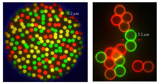
I was fortunate to work in the nanotech field in graduate school. During this time, I investigated and developed methods for forming ceramic composites, which maintain a nanoscale grain size even after sintering. Sintering is the process used to form fully dense ceramic materials. The problem with sintering is that it adds energy to a system, resulting in grain growth of the ceramic materials. In order to maintain the advantageous properties of the nanosized grains, I worked on methods that pinned the ceramic grain boundaries to reduce growth during sintering.

The methods I developed not only involved handling of nanosized ceramic particles, but also the deposition of nanofilms into a porous ceramic material to create nanocomposites. I have been able to apply this experience in my IP practice to assist clients in obtaining and assessing IP in the areas of nanolaminates and coatings, nanosized particles and nanostructures, such as carbon nanotubes, nano fluidic devices, which are very small devices which transport fluids, and 3D structures formed from nanomaterials, such as woven nanofibers.

Editor: I understand that some of the components of the new Boeing 787 are examples of nanotechnology.

Vernon: The design objective behind the 787 is that lighter, better-performing materials will reduce the weight of the aircraft, resulting in longer possible flight times and decreased operating costs. Boeing reports that approximately 50 percent of the materials in the 787 are composite materials, and that nanotechnology will play an important role in achieving and exceeding the design objective. (See, http://www.nasc.com/nanometa/Plenary%20Talk%20Chong.pdf).

While it is believed that nanocomposite materials are used in the fuselage of the 787, Boeing is investigating applying nanotechnology to reduce costs and increase performance not only in fuselage and aircraft structures, but also within energy, sensor and system controls of the aircraft.

Editor: What products have incorporated nanotechnology? What products are anticipated to incorporate its processes in the future?

Vernon: The products that people are the most familiar with are cosmetic products, such as hair products for thinning hair that deliver nutrients deep into the scalp, and sunscreen, which includes nanosized titanium dioxide and zinc oxide to eliminate the white, pasty look of sunscreens. Sports products, such as fishing rods and tennis rackets, have incorporated a composite of carbon fiber and silica nanoparticles to add strength. Nano products are used in paints and coatings to prevent algae and corrosion on the hulls of boats and to help reduce mold and kill bacteria. We’re seeing nanotechnology used in filters to separate chemicals and in water filtration.

The textile industry has also started to use nano coatings to repel water and make fabrics flame resistant. The medical imaging industry is starting to use nanoparticles to tag certain areas of the body, allowing for enhanced MRI imaging. Developing areas include drug delivery, disease detection and therapeutics for oncology. Obviously, those are definitely in the future, but it is the direction of scientific thinking.

Editor: What liabilities can product manufacturers incur who are incorporating nanotechnology into their products? What kinds of health and safety risks are incurred in their manufacture or consumption?Nano Body II 43a262816377a448922f9811e069be13

Vernon: There are three different areas that we should think about: the manufacturing process, consumer use and environmental issues. In manufacturing there are potential safety issues with respect to the incorporation or delivery of nanomaterials. For example, inhalation of nanoparticles can cause serious respiratory issues, and contact of some nanoparticles with the skin or eyes may result in irritation. In terms of consumer use, nanomaterials may have different material properties from their larger counterparts.

As a result, we are not quite sure how these materials will affect the human body insofar as they might have a higher toxicity level than in their larger counterparts. With respect to an environmental impact, waste or recycled products may lead to the release of nanoparticles into bodies of water or impact wildlife. The National Institute for Occupational Safety and Health has established the Nanotechnology Research Center to develop a strategic direction with respect to occupational safety and nanotechnology. Guidance and publications can be found at http://www.cdc.gov/niosh/topics/nanotech.

Editor: The European Union requires the labeling of foods containing nanomaterials. What has been the position of the Food & Drug Administration and the EPA in the United States about food labeling?

Vernon: So far the FDA has taken the position that just because nanomaterials are smaller, they are not materially different from their larger counterparts, and therefore there have been no labeling requirements on food products. The FDA believes that their current standards for safety assessment are robust and flexible enough to handle a variety of different materials. That being said, the FDA has issued some guidelines for the food and cosmetic industries, but there has not been any requirement for food labeling as of now. The EPA has a nanotechnology division, which is also studying nanomaterials and their impact, but I haven’t seen anything that specifically requires a special registration process for nanomaterials.

Editor: What new regulations regarding nanotech products are expected? Should governmental regulations be adopted to prevent nanoparticles in foods and cosmetics from causing toxicity?

Vernon: The FDA has not telegraphed that any new regulations will be put into place. The agency is currently in the data collection stage to make sure that these materials are being safely delivered to people using current FDA standards – that materials are safe for human consumption or contact with humans. We won’t really understand whether or not regulations will be coming into place until we see data coming out that indicates that there are issues that are directly associated with nanomaterials. Rather than expecting regulations, I would suggest that we examine the data regarding nano products to optimize safe handling and use procedures.

Editor: Have there ever been any cases involving toxicity resulting from nano products?

Vernon: There are current investigations about the toxicity of carbon nano tubes, but the research is in its infancy. There is no evidence to show any potential harm from this technology. Unlike asbestos or silica exposure, the science is not there yet to demonstrate any toxicity link. The general understanding is that it may take decades for any potential harm to manifest. I believe my colleague, Patrick J. Comerford, head of McCarter’s product liability team in Boston, summarizes the situation well by noting that “if any supportable science was available, plaintiff’s bar would have already made this a high-profile target.”

Editor: While some biotech cases have failed the test of patentability before the courts, such as the case of Mayo v. Prometheus, what standard has been set forth for a biotech process to pass the test for patentability?

Vernon: There is no specified bright-line test for determining if a biotech process is patentable. But what the U.S. Patent and Trademark Office has done is to issue some new examination guidelines with respect to the Mayo decision that help examiners figure out whether a biotech process is patent eligible. Specifically, the guidelines look to see if the biotech process (i.e., a process incorporating a law of nature) also includes at least one additional element or step. That additional element needs to be significant and not just a mental or correlation step. If a biotech process patent claim includes this significant additional step, there still needs to be a determination if the process is novel and non-obvious over the prior art. So while this might not be a bright-line test to help us figure out whether a biotech process is patentable, it at least gives us some direction about what the examiners are looking for in the patent claims.

Editor: What effect do you think the new America Invents Act will have in encouraging biotech companies to file early in the first stages of product development? Might that not run the risk that the courts could deny patentability as in the Ariad case where functional results of a process were described rather than the specific invention?

Vernon: The AIA goes into effect next month. What companies, especially biotech companies, need to do is file early. Companies need to submit applications supported by their research to include both a written description and enablement of the invention. Companies will need to be more focused on making sure that they are not only inventing in a timely manner but are also involving their patent counsel in planned and well-thought-out experiments to make sure that the supporting information is available in a timely fashion for patenting.

Editor: Have there been any recent cases relating to biotechnology or nanotechnology that our readers should be informed about?

Vernon: The Supreme Court will hear oral arguments in April in the Myriad case. This case involves the BRCA gene, the breast cancer gene – and the issue is whether isolating a portion of a gene is patentable. While I am not a biotechnologist, I think this case will also impact nanotechnology as a whole. Applying for a patent on a portion of a gene is not too far distant from applying for a patent on a nanoparticle of a material that already exists but which has different properties from the original, larger-counterpart material. Would this nanosize material be patentable? This will be an important case to see what guidance the Supreme Court delivers this coming term.

Editor: Is there anything else you’d like to add?

Vernon: I think the next couple of years for nanotech will be very interesting. As I mentioned, I did my PhD thesis in the nanotechnology area a few years ago. My studies, like those of many other students, were funded in part with government grants. There is a great deal of government money being poured into nanotechnology. In the next ten years we will start seeing more and more of this research being commercialized and adopted into our lives. To keep current of developments, readers can visit www.nano.gov.

The Metropolitan Corporate Counsel
The Leading Resource For Corporate Counsel

As a leading publication in the corporate counsel community, MCC offers unique editorial content covering legal, regulatory, legislative and business developments, featuring original articles and interviews from experts at prestigious law firms, bar associations, accounting firms and legal service providers, as well as educators, business executives and high-level state, national and international officials.


Peptoid Nanosheets at the Oil/Water Interface


Peptides Ron-Zuckerman-nanosheets-300x156Berkeley Lab Reports New Route to Novel Family of Biomimetic Materials


From the people who brought us peptoid nanosheets that form at the interface between air and water, now come peptoid nanosheets that form at the interface between oil and water. Scientists at the U.S. Department of Energy (DOE)’s Lawrence Berkeley National Laboratory (Berkeley Lab) have developed peptoid nanosheets – two-dimensional biomimetic materials with customizable properties – that self-assemble at an oil-water interface. This new development opens the door to designing peptoid nanosheets of increasing structural complexity and chemical functionality for a broad range of applications, including improved chemical sensors and separators, and safer, more effective drug delivery vehicles.

“Supramolecular assembly at an oil-water interface is an effective way to produce 2D nanomaterials from peptoids because that interface helps pre-organize the peptoid chains to facilitate their self-interaction,” says Ron Zuckermann, a senior scientist at the Molecular Foundry, a DOE nanoscience center hosted at Berkeley Lab. “This increased understanding of the peptoid assembly mechanism should enable us to scale-up to produce large quantities, or scale- down to screen many different nanosheets for novel functions.”


Ron Zuckerman and Geraldine Richmond led the development of peptoid nanosheets that form at the interface between oil and water, opening the door to increased structural complexity and chemical functionality for a broad range of applications.

Zuckermann, who directs the Molecular Foundry’s Biological Nanostructures Facility, and Geraldine Richmond of the University of Oregon are the corresponding authors of a paper reporting these results in the Proceedings of the National Academy of Sciences (PNAS). The paper is titled “Assembly and molecular order of two-dimensional peptoid nanosheets at the oil-water interface.” Co-authors are Ellen Robertson, Gloria Olivier, Menglu Qian and Caroline Proulx.

Peptoids are synthetic versions of proteins. Like their natural counterparts, peptoids fold and twist into distinct conformations that enable them to carry out a wide variety of specific functions. In 2010, Zuckermann and his group at the Molecular Foundry discovered a technique to synthesize peptoids into sheets that were just a few nanometers thick but up to 100 micrometers in length. These were among the largest and thinnest free-floating organic crystals ever made, with an area-to-thickness equivalent of a plastic sheet covering a football field. Just as the properties of peptoids can be chemically customized through robotic synthesis, the properties of peptoid nanosheets can also be engineered for specific functions.

“Peptoid nanosheet properties can be tailored with great precision,” Zuckermann says, “and since peptoids are less vulnerable to chemical or metabolic breakdown than proteins, they are a highly promising platform for self-assembling bio-inspired nanomaterials.”

In this latest effort, Zuckermann, Richmond and their co-authors used vibrational sum frequency spectroscopy to probe the molecular interactions between the peptoids as they assembled at the oil-water interface. These measurements revealed that peptoid polymers adsorbed to the interface are highly ordered, and that this order is greatly influenced by interactions between neighboring molecules.

“We can literally see the polymer chains become more organized the closer they get to one another,” Zuckermann says.

Peptoid polymers adsorbed to the oil-water interface are highly ordered thanks to interactions between neighboring molecules.

The substitution of oil in place of air creates a raft of new opportunities for the engineering and production of peptoid nanosheets. For example, the oil phase could contain chemical reagents, serve to minimize evaporation of the aqueous phase, or enable microfluidic production.

“The production of peptoid nanosheets in microfluidic devices means that we should soon be able to make combinatorial libraries of different functionalized nanosheets and screen them on a very small scale,” Zuckermann says. “This would be advantageous in the search for peptoid nanosheets with the molecular recognition and catalytic functions of proteins.”

Zuckermann and his group at the Molecular Foundry are now investigating the addition of chemical reagents or cargo to the oil phase, and exploring their interactions with the peptoid monolayers that form during the nanosheet assembly process.

“In the future we may be able to produce nanosheets with drugs, dyes, nanoparticles or other solutes trapped in the interior,” he says. “These new nanosheets could have a host of interesting biomedical, mechanical and optical properties.”

This work was primarily funded by the DOE Office of Science and the Defense Threat Reduction Agency. Part of the research was performed at the Molecular Foundry and the Advanced Light Source, which are DOE Office of Science User Facilities.

Additional Information

For more about the research of Ronald Zuckermann go here

For more about the research of Geraldine Richmond go here

For more about the Molecular Foundry go here

#  #  #

Lawrence Berkeley National Laboratory addresses the world’s most urgent scientific challenges by advancing sustainable energy, protecting human health, creating new materials, and revealing the origin and fate of the universe. Founded in 1931, Berkeley Lab’s scientific expertise has been recognized with 13 Nobel prizes. The University of California manages Berkeley Lab for the U.S. Department of Energy’s Office of Science.  For more, visit www.lbl.gov.

– See more at: http://newscenter.lbl.gov/2014/09/03/peptoid-nanosheets-at-the-oilwater-interface/#sthash.61uDiBBR.dpuf

Researchers Intoduce an Electric Field to Enhance Solar Cell Performance


Electrical Field pic1Researchers at the Kavli Energy Nanosciences Institute, the University of California at Berkeley and the Lawrence Berkeley National Lab, have succeeded in boosting the performance of a new type of solar cell by simply applying an electric field to it. The device (made of low cost zinc phosphide and graphene) is novel in its design in that it lacks a junction between the two p- and n-type semiconductors that make it up – which is a first. The cell might be ideal for use in areas where the intensity of sunlight changes a lot over the course of the year.

The device and experimental results

“Our solar cell does not need to be doped, nor does it require high-quality heterojunctions, which are challenging and expensive to fabricate,” says team member Oscar Vazquez-Mena. “Our work is a novel and promising approach for making photovoltaics with low-cost and abundant materials such as certain phosphides and sulphides that are easy to synthesize and which are environmentally friendly.”

Beside expensive light absorbers like silicon, there are semiconductors like zinc phosphide, copper zinc tin sulphide, cuprous oxide and iron sulphide that are much cheaper. However, for these materials to efficiently convert sunlight into energy, they need to be doped to form homojunctions, or require complementary emitter materials to form high-quality p-n heterojunctions.

A team led by Alex Zettl, Harry Atwater, Ali Javey and Michael Crommie has now overcome this problem by making a simple junction with graphene rather than a semiconductor. A voltage applied to a gate over the junction can tune the energy barrier between the graphene and an adjoining layer of zinc phosphide to boost how efficiently solar cells made from these materials convert light into energy.

The devices are relatively simple to fabricate, says Vazquez-Mena. “Jeff Bosco from Harry Atwater’s team at Caltech makes high-quality zinc phosphide films and in our lab at UC Berkeley, we are experts at growing graphene on copper substrates. Basically, we transfer the graphene from the copper onto the zinc phosphide film to form a graphene- zinc phosphide junction. We then add an insulator layer on top of the graphene, prepared by our colleagues in Ali Javey’s team, also at UC Berkeley. Finally we add a thin top gate to the structure.”

Barrier is like a dam

Conventional solar cells normally contain two bulk semiconductors, with their electrons at different energy levels. These semiconductors are brought into contact to form an electric barrier between them that separates the electrons from each side. “This barrier can be likened to the dam in a hydroelectric power plant that separates two reservoirs of water at different heights,” explains Vazquez-Mena. “In a solar cell, the electric charges are the water in the dam and we use energy from the Sun to make the charges jump over the barrier.”

In the new device, the researchers used a layer of graphene in place of one of the semiconductors and added a top gate to it. “Why? Because it is easy to control the energy level of electrons in graphene by doing this,” Vazquez-Mena tells nanotechweb.org. “Such a thing is difficult to do in a bulk semiconductor.”

The top gate can regulate the barrier between graphene and the zinc phosphide, needed for the solar cell to work, he adds. “This is critical for the performance of the device and allows us to optimize the energy extracted from it. Going back to the dam analogy, it is as if we would be controlling the height of the dam.”

The fact that we can manipulate the barrier height in this way means that, in principle, we could make graphene junctions with many other materials, he says.

Modifying the barrier

In bulk semiconductor solar cells, the barrier height depends on the intrinsic properties of the materials making up the barrier. So, once you put the materials together, there is not much you can do to change the barrier, explains Vazquez-Mena.

“Our device is very different in that we can modify this barrier by simply applying an electric field to the top gate and adjusting the strength of the field applied for different materials and light conditions to optimize energy conversion. Our device, which is just a basic graphene-zinc phosphide solar cell, normally has an efficiency of 1% without any applied gate voltage, but we have doubled this to 2% by increasing the gate voltage to 2V. We have thus been able to boost its performance beyond the intrinsic properties of the material it is made up of.”

This type of solar cell might be ideal in climes where the sunlight varies a lot, he says – thanks to the fact that we can adjust the barrier to optimize energy conversion.

The California researchers say that they are looking to improve the efficiency of their devices and improving the quality of the graphene-zinc phosphide junction so that it produces a higher photocurrent. “We also want to apply our technology to other low-cost and readily available materials,” says Vazquez-Mena. “For example, the device we have made can be improved by using graphene itself or a transparent conductor like indium-tin oxide as the top gate.”

The team, reporting its work in Nano Letters, says that it will also test copper zinc tin sulphide, cuprous oxides and copper sulphide. “These materials are less harmful to the environment compared with commonly used solar cell materials like cadmium telluride and are cheaper than pure silicon. We definitely have many ideas to try but we also hope that other research groups will be inspired by our experiments and develop similar strategies to keep improving the efficiencies of alternative photovoltaic materials.”

Genesis Nanotech Headlines Are Out!


Organ on a chip organx250Genesis Nanotech Headlines Are Out! Read All About It!

https://paper.li/GenesisNanoTech/1354215819#!headlines

Visit Our Website: www.genesisnanotech.com

Visit/ Post on Our Blog: https://genesisnanotech.wordpress.com


SUBCOMMITTE EXAMINES BREAKTHROUGH NANOTECHNOLOGY OPPORTUNITIES FOR AMERICA

Chairman Terry: “Nanotech is a true science race between the nations, and we should be encouraging the transition from research breakthroughs to commercial development.”

WASHINGTON, DCThe Subcommittee on Commerce, Manufacturing, and Trade, chaired by Rep. Lee Terry (R-NE), today held a hearing on:

“Nanotechnology: Understanding How Small Solutions Drive Big Innovation.”


electron-tomography

“Great Things from Small Things!” … We Couldn’t Agree More!


Quantum Dots may turn House Windows into Solar Panels


New-QD-Solar-Cell-id35756-150x150A house window that doubles as a solar panel could be on the horizon, thanks to recent quantum-dot work by researchers at Los Alamos National Laboratory in the US in collaboration with scientists from University of Milano-Bicocca (UNIMIB) in Italy.

Their work, published earlier this year in Nature Photonics, demonstrates that superior light-emitting properties of quantum dots can be applied in solar energy by helping more efficiently harvest sunlight.

“The key accomplishment is the demonstration of large-area luminescent solar concentrators that use a new generation of specially engineered quantum dots,” said lead researcher Victor Klimov of the Center for Advanced Solar Photophysics at Los Alamos. Quantum dots are ultra-small bits of semiconductor matter that can be synthesized with nearly atomic precision via modern methods of colloidal chemistry.

A luminescent solar concentrator (LSC) is a photon-management device, representing a slab of transparent material that contains highly efficient emitters such as dye molecules or quantum dots. Sunlight absorbed in the slab is re-radiated at longer wavelengths and guided toward the slab edge equipped with a solar cell.

Quantum dots are embedded in the plastic matrix and capture sunlight to improve solar-panel efficiency.
Courtesy Los Alamos Lab.
 
LUMINESCENT SOLAR CONCENTRATOR AS LIGHT HARVESTER

Sergio Brovelli, a faculty member at UNIMIB and a co-author of the paper, explained, “The LSC serves as a light-harvesting antenna which concentrates solar radiation collected from a large area onto a much smaller solar cell, and this increases its power output. LSCs are especially attractive because in addition to gains in efficiency, they can enable new interesting concepts such as photovoltaic windows that can transform house facades into large-area energy-generation units.”

Because of highly efficient, color-tunable emission and solution processability, quantum dots are attractive materials for use in inexpensive, large-area LSCs. To overcome a nagging problem of light reabsorption, the Los Alamos and UNIMIB researchers developed LSCs based on quantum dots with artificially induced large separation between emission and absorption bands, known as a large Stokes shift.

These “Stokes-shift-engineered” quantum dots represent cadmium selenide/cadmium sulfide (CdSe/CdS) structures in which light absorption is dominated by an ultra-thick outer shell of CdS, while emission occurs from the inner core of a narrower-gap CdSe.

Los Alamos researchers created a series of thick-shell (so-called “giant”) CdSe/CdS quantum dots, which were incorporated by their Italian partners into large slabs (sized in tens of centimeters across) of polymethylmethacrylate. While being large by quantum dot standards, the active particles are still tiny, only about hundred angstroms across.

QUANTUM DOTS USED FOR NEW DISPLAYS

Quantum dots are ultra-small bits of semiconductor matter that can be synthesized with nearly atomic precision via modern methods of colloidal chemistry.

Their emission color can be tuned by simply varying their dimensions. Color tunability is combined with high emission efficiencies approaching 100%.3D Printing dots-2

These properties have recently become the basis of a new technology — quantum-dot displays — employed, for example, in the newest generation of the Kindle Fire e-reader.

In a new SPIE.TV video, Lawrence Berkeley National Lab director Paul Alivisatos demonstrates the Kindle Fire quantum-dot display.


DOI: 10.1117/2.4201407.10

Breakthrough Method (Discovery) for Characterizing Hot Carriers Could Hold the Key to Future Solar Cell Efficiencies


XBD200209-00526-02.PSDOne of the major road blocks to the design and development of new, more efficient solar cells may have been cleared. Researchers with the Lawrence Berkeley National Laboratory (Berkeley Lab) have developed the first ab initio method – meaning a theoretical model free of adjustable or empirical parameters – for characterizing the properties of “hot carriers” in semiconductors. Hot carriers are electrical charge carriers – electrons and holes – with significantly higher energy than charge carriers at thermal equilibrium.

“Hot carrier thermalization is a major source of efficiency loss in solar cells, but because of the sub-picosecond time scale and complex physics involved, characterization of hot carriers has long been a challenge even for the simplest materials,” says Steven Louie, a theoretical physicist and senior faculty scientist with Berkeley Lab’s Materials Sciences Division (MSD). “Our work is the first ab initio calculation of the key quantities of interest for hot carriers – lifetime, which tells us how long it takes for hot carriers to lose energy, and the mean free path, which tells us how far the hot carriers can travel before losing their energy.”

XBD200209-00526-02.PSD

A new and better way to study “hot” carriers in semiconductors, a major source of efficiency loss in solar cells, has been developed by scientists at Berkeley Lab. (Photo by Roy Kaltschmidt)

All previous theoretical methods for computing these values required empirical parameters extracted from transport or optical measurements of high quality samples, a requirement that among the notable semiconductor materials has only been achieved for silicon and gallium arsenide. The ab initio method developed by Louie and Jeff Neaton, Director of the Molecular Foundry, a U.S. Department of Energy (DOE) Nanoscience User Facility hosted at Berkeley Lab, working with Marco Bernardi, Derek Vigil-Fowler and Johannes Lischner, requires no experimental parameters other than the structure of the material.

(From left) Steve Louie, Marco Bernardi, Jeff Neaton and Johannes Lischner developed the first ab initio method for characterizing hot carriers in semiconductors. (Photo by Roy Kaltschmidt)

“This means that we can study hot carriers in a variety of surfaces, nanostructures, and materials, such as inorganic and organic crystals, without relying on existing experiments,” says Neaton. “We can even study materials that have not yet been synthesized. Since we can access structures that are ideal and defect-free with our methods, we can predict intrinsic lifetimes and mean free paths that are hard to extract from experiments due to the presence of impurities and defects in real samples. We can also use our model to directly evaluate the influence of defects and impurities.”

Neaton, like Louie, is a senior MSD faculty scientist with the University of California (UC) Berkeley. Neaton also holds an appointment with the Kavli Institute for Energy Nanosciences. They are the corresponding authors of a paper in Physical Review Letters describing this work titled “Ab Initio Study of Hot Carriers in the First Picosecond after Sunlight Absorption in Silicon.” Bernardi is the lead author of the paper, and Vigil-Fowler the primary coauthor.

Single-junction solar cells based on crystalline silicon are rapidly approaching the theoretical limit of their efficiency, which is approximately 30-percent. This means that if a silicon-based solar cell collects 1,000 Watts per square meter of energy, the most electricity it can generate is 300 Watts per square meter. Hot carriers are crucial to enhancing solar cell  efficiency, since their thermalization results in the loss of as much as a third of the absorbed solar energy in silicon, and similar values in other semiconductors. However, the properties of hot carriers in complex materials for photovoltaic and other modern optoelectronic applications are still poorly understood.

“Our study was aimed at providing useful data for hot carrier dynamics in silicon with application in solar cells,” says Bernardi. “In this study we provide calculations from first principles that describe the two key loss mechanisms, induced by electrons and phonons, respectively, with state-of-the-art accuracy and within the frameworks of density functional and many-body perturbation theories.”

When the research team applied their method to study the relaxation time and mean free path of hot carriers in silicon, they found that thermalization under solar illumination is completed within 350 femtoseconds, and is dominated by phonon emission from hot carriers, a process that becomes progressively slower as the hot carriers lose energy and relax toward the band edges. This modeling result was in excellent agreement with the results of pump-probe experiments. While the model was only tested on silicon in this study, the researchers are confident it will be equally successful with other materials.

“We believe our approach is highly valuable to experimental groups studying hot carriers in the context of solar cells and other renewable energy technologies as it can be used to compute the lifetime and mean free path of hot carriers with specific energies, momenta, and crystallographic directions with unprecedented resolution,” Bernardi says. “As we expand our study of hot carriers to a range of crystalline materials and nanostructures, we believe that our data will provide unique microscopic insight to guide new experiments on hot carriers in semiconductors.”

This research was supported by the DOE Office of Science and the National Science Foundation and made use of the Molecular Foundry, as well as computational resources of the National Energy Research Scientific Computing Center (NERSC), which is also supported by the DOE Office of Science.

Additional Information

For more about the research of Steven Louie go here

For more about the research of Jeff Neaton go here

For more about the Molecular Foundry go here

For more about NERSC go here

For more about the Kavli Institute for Energy Nanosciences go here

– See more at: http://newscenter.lbl.gov/2014/07/17/first-ab-initio-method-for-characterizing-hot-carriers/#sthash.wY178h9s.dpuf