BASF increased spending on research and development to €1.8 billion (2012: €1.7 billion) in 2013. “In absolute terms, we lead the field in the chemical industry with our research and development expenditures,” said Dr. Andreas Kreimeyer, member of the Board of Executive Directors of BASF SE and Research Executive Director, at the Research Press Conference on the topic ”Nanotechnology: Small dimensions – great opportunities” in Ludwigshafen.
BASF has a workforce of around 10,650 employees working in international and interdisciplinary teams on around 3,000 research projects to find answers to the challenges of the future and secure sustainable profitable growth for the company.
The innovative strength of BASF is demonstrated once more by sales of new products introduced onto the market within the past five years: Last year these amounted to about €8 billion. In 2013 alone, the company launched more than 300 new products on the market. The patent portfolio also reflects the success of the company’s research activities. With 1,300 patents filed last year and about 151,000 registrations and intellectual property rights worldwide, BASF is at the top of the Patent Asset Index for the fifth time in succession.
New research laboratories in North America and Asia
In future, BASF is expecting strong impulses from the regions for its innovation pipeline. By 2020, 50% of its research activities are to be conducted outside Europe. In 2013, BASF came another step closer to this goal and increased the proportion of its research outside Europe to 28% (2012: 27%). To drive the globalization of research further forward, the company has, among other things, established six new laboratories at different locations in Asia and the United States. Moreover, for example in cooperation with highly innovative universities, BASF has founded the “California Research Alliance by BASF” (CARA) in California. Here, the main research focus is on the biosciences and new inorganic materials for the areas energy, electronics and renewable resources. In Asia, the company has, for example, joined forces with top-ranking universities from China, Japan and Korea to found the research initiative ”Network for Advanced Materials Open Research” (NAO). In this joint project, research is underway on materials for a wide range of applications, including products for the automotive, construction and water industries and for the wind energy sector.
BASF collaborates in a global network with more than 600 outstanding universities, research institutes and companies. “Interdisciplinary and international cooperations are a decisive element of BASF’s Know-how Verbund,” added Kreimeyer. Offering intelligent solutions for the challenges of the future based on new systems and functional materials requires not only interdisciplinary approaches but also the use of cross-sectional technologies like nanotechnology.
Nanotechnology – helping to develop solutions for the future
Nanotechnology is concerned with the development, manufacture and use of materials that have structures, particles, fibers or platelets smaller than 100 nanometers and so possess novel properties. Many innovations in areas such as automotive technology, energy, electronics or construction and medicine would not be possible without nanotechnology. BASF uses this technology to develop new solutions and improve existing products.
High-performance insulation materials
Nanopores provide the specific material characteristics in one of BASF’s new high-performance insulation material. Slentite™ is the first high-performance insulation panel based on polyurethane, which needs only half the space compared to traditional materials while offering the same insulation performance. Up to 90% of the volume of the organic aerogel consists of air-filled pores which have a diameter of only 50 to 100 nanometers. As a result, the air molecules’ freedom of movement is limited and the transfer of heat is reduced. The high-performance insulation material can be used, for example, in the construction sector for old and new buildings.
Microencapsulation
One BASF research field in which nanotechnology plays a key role focuses on the development of formulations of active components, especially on microencapsulation. Active substances are thereby enclosed with a wax, polymer or oil-based protective shell. This enables the actives to be used more specifically for the application concerned and function more effectively. The important factor here is the controlled release of the actives. Researchers at BASF have succeeded in designing the shell according to the application need, making it only a few nanometers thick or nanostructured. This allows control of the time and speed at which the active substances can be released at the desired target location.
A material that could contribute to the key technological progress of Organic Light Emitting Diodes (OLEDs), displays and even batteries and catalysts is graphene. It is closely related to graphite, which is used, for example, in pencil leads. Unlike graphite, graphene consists of only one layer of carbon atoms, making it less than one nanometer thin. This material is a very efficient electricity and heat conductor and is very stable but also elastic and flexible. Because it is so thin, the actually black material appears transparent. An international team of researchers is currently exploring the scientific basis and application potential of innovative carbon-based materials like graphene at the joint research and development platform of BASF and the Max Planck Institute for Polymer Research in Mainz, Germany.
Color filters
BASF’s new red color, Irgaphor® Red S 3621 CF, ensures an excellent image quality of liquid crystal displays (LCD). It is used in color filters for notebook, computer and television screens. The smaller the particles are, the more intense the brightness of screens becomes. BASF has succeeded in manufacturing its product with a particle size of less than 40 nanometers. The tiny particles enable considerably less scattering of light in the color filter. Compared to traditional color products, BASF’s new red doubles the contrast ratio of displays. This leads to a sharp, pure-colored, high-contrast and thus brilliant image.
Safely utilizing the potentials of nanotechnology
Accessing new technologies requires an objective assessment of both the opportunities and risks. In addition to the manufacture and development of nanomaterials, another research priority is the risk assessment of nanoparticles. For about ten years, BASF has therefore been pursuing safety research with nanomaterials. During this time the company has conducted more than 150 own toxicology and ecotoxicology studies and participated in approximately 30 different projects with external partners.
Open dialog for a common understanding
Innovation-friendly social and political conditions are decisive in allowing the potentials of nanotechnology to be utilized. “Public discussion is very important for us. We actively seek dialog, also with critical opinion leaders,” said Kreimeyer. For example, BASF has – as the first and so far only company in Germany – established a regularly held dialog forum focusing on nanotechnology. At these events, BASF employees conduct discussions with various representatives of environmental and consumer organizations, labor unions, scientific institutions and churches to improve understanding of current concerns, explain opportunities, answer questions and jointly identify constructive solutions.
About BASF
BASF is the world’s leading chemical company: The Chemical Company. Its portfolio ranges from chemicals, plastics, performance products and crop protection products to oil and gas. We combine economic success with environmental protection and social responsibility. Through science and innovation, we enable our customers in nearly every industry to meet the current and future needs of society. Our products and solutions contribute to conserving resources, ensuring nutrition and improving quality of life. We have summed up this contribution in our corporate purpose: We create chemistry for a sustainable future. BASF had sales of about €74 billion in 2013 and over 112,000 employees as of the end of the year. Further information on BASF is available on the Internet at http://www.basf.com.
One of the most heavily used materials for water purification filters is carbon, usually in the form of activated carbon – i.e. carbon treated with oxygen to open up microscopic pores).
This high degree of porosity and the resulting high surface area make this material ideal, among other things, for removing pollutants (that are attracted to carbon, such as volatile organic compounds, pesticides and benzene) from water.
One of the problems with activated carbon is the disposal of adsorbed contaminants along with the adsorbent. Another concern is that its pores are often blocked during adsorption. By contrast, carbon nanotubes’ (CNTs) open structure offers easy, undisrupted access to reactive sites located on nanotubes’ outer surface.
That’s why researchers see CNTs as an attractive potential substitute for activated carbon (see for instance: “Smart capsules for water treatment with recyclable carbon nanotube cores”). “An issue with using CNTs for water purification of course is the fact that unbounded nanotubes would pose health risks to humans and the ecosystem because they are difficult to separate from treated water,” Chongzheng Na, an Assistant Professor in the Department of Civil and Environmental Engineering and Earth Sciences at the University of Notre Dame, tells Nanowerk.
Na says that the challenge of improving CNTs separability has been tackled by other researchers in the past. “The motivation is to eliminate an important concern regarding the use of CNTs for water purification, namely how the CNTs will be collected after treatment. From an application point of view, a high efficiency of recollection is important for cost saving. From a health point of view, a high efficiency of recollection eliminates concerns of potential harms that loose CNTs may do to humans and ecosystems.”
In new work published in the May 7, 2014 online edition of ACS Applied Materials & Interfaces (“Multifunctional and Recollectable Carbon Nanotube Ponytails for Water Purification”), Na, postdoc fellow Haitao Wang, and graduate student Hanyu Ma, have demonstrated that individual CNTs can be integrated into micrometer-sized colloidal particles without using a heavy or bulky particulate support. Organizing individual nanotubes into hierarchical structures represents a new strategy to scale up nanomaterials for macroscopic engineering applications. The researchers grew CNT arrays of hundreds of micrometers in length on nanometer-thin mineral discs with a negligible mass and volume, a structure they termed carbon nanotube ponytails (CNPs).
The layered double oxide (LDO) discs are slightly magnetic. This magnetization is sufficiently weak to prevent CNPs from aggregating under self-attraction but strong enough to be utilized for separation. “Compared to individual CNTs, CNPs can be more effectively separated from water using gravitational sedimentation, magnetic attraction, and membrane filtration while having the ability to perform adsorption, disinfection, and catalytic degradation of contaminants in water”, explains Na.
Schematic of water purification with carbon nanotube ponytails. (Image: Xia Zhao and Na Lab, University of Notre Dame)
To address the CNT separability issue, researchers previously did the same thing as Na’s team, i.e. increase the overall size of CNTs. For example, CNTs were fixed on inactive colloidal particles. What makes the CNT ponytails special, though, is that they contain little supporting material. An interesting aspect from a material synthesis point of view is that this work demonstrates the preparation of CNT colloidal particles nearly free of support without involving exotic procedures – i.e., CNPs are made using the same standard chemical vapor deposition method for CNT growth using a slightly different catalyst material.
“The elimination of extensive use of support transforms CNT colloids from a composite material containing only a minor mass/volume fraction of the active component (i.e., CNTs) to a material almost exclusively made of active CNTs,” says Na. “Obvious advantages include saving energy for transportation and saving space in use.”
In their water purification experiments, the researchers showed that their CNPs are as good as CNTs for removing contaminants from water as adsorbents, disinfectants, and catalyst supports. Unlike unbounded CNTs, as Na points out, CNPs can be separated more effectively using common techniques such as gravitational sedimentation, magnetic attraction, and membrane filtration.
For water purification, processes using CNPs might be helpful in situations where commonly used water treatment infrastructures are not available, for instance, providing clean water in developing countries or remote rural areas. In addition, CNPs can be used in industrial processes – e.g., as catalyst supports – and emergency response, e.g., adsorbents for chemical spills.
Going forward, the team would like to further reduce the cost of making multifunctional and recollectable hierarchical materials for water purification so that the treatments described in their paper can become more affordable. “Obviously” says Na, “this would be tied to the advancement of CNT synthesis if we keep using CNTs as the building material. Alternatively, we are looking into materials that are less expensive than CNTs. Our study with CNPs has provided insights for what properties we should be looking for in the alternative materials.”
Given the recent advances in nanotechnology, the water community has been searching for ways to incorporate nanomaterials into treatment processes. There is, however, a tremendous dimensional disparity between the nano world and the water world. No one is interested in nanoliters of water. When people talk about water, they talk in units such as million gallons per day. The challenge is how to connect these two worlds on the dimension ladder.
“What we did in making CNPs has done precisely that,” says Na. “By integrating nanotubes into colloidal particles, we helped CNTs climb from the nanometer rung to the micrometer rung on the dimension ladder. By incorporating magnetism into CNPs, we elevated CNTs even further to the centimeter scale.” “In our future research, we will keep looking for better ways to connect nanomaterials to the world that we live in – in technical terms, we will be researching for new strategies to scale up nanoscale properties for water purification,” he concludes.
From solar panels to batteries, algorithms are becoming key to designing new materials
Summary: Materials science is being transformed by algorithms, and computers are now selecting new material combinations to test in the lab.
In the future, materials that could make a super efficient solar panel or a breakthrough battery probably won’t be discovered by a smart human scientist. Like everything else in this world, computers and software are increasingly identifying the best combination of materials to deliver a desired result, and then human researchers are testing out those computers’ choices in the lab.
For University of Colorado professor Alex Zunger, that idea is a fundamental change in materials research. Zunger is the chief theorist at the Center for Inverse Design, and at the SunShot Summit last week he spoke about how “inverse design” — identifying specific properties that are desired in a material, then determining that material’s required atomic structure — could transform sectors like solar.
For decades, materials for new applications have been selected to be tested “rather casually,” said Zunger, based on “simple ideas,” or even “availability in the lab.” But now, thanks to sophisticated algorithms, scientists can use computer intelligence to make these choices.
Zunger is particularly interested in using inverse design and computer intelligence to figure out the optimal materials to use quantum dots for solar materials. Quantum dots are little pieces of semiconductor crystals — less than 10 nanometers — that are so small they have different properties and characteristics than larger semiconductor pieces. But so far, Zunger says, there hasn’t been an obvious winning combination for solar quantum dots.
Zunger isn’t the only one doing this. It’s actually a hot trend for some of the most cutting-edge materials startups out there.
For example, a startup called Pellion Technologies, which was spun out of MIT, developed advanced algorithms and computer modeling that enabled it to test out 10,000 potential cathode materials to fit with a magnesium anode for a battery. Now the startup is developing a magnesium battery, which could have a very high energy density, and if it works could be important for electric vehicles and grid storage.
A founder of Pellion, MIT professor Gerbrand Ceder, helped develop the Materials Genome Project at MIT, which is a program that uses computer modeling and virtual simulations to deliver innovation in materials. The Economist once described Ceder’s work with the Materials Genome Project as “a short cut” for discovering electrodes and the interactions of inorganic chemical compounds.
Other smart people are also working on this idea. Columbia University’s Institute for Data Sciences and Engineering spearheaded important work in the area, and professors Venkat Venkatasubramanian and Sanat Kumar recently published research on their work designing nanostructured materials with an inverse design framework and genetic algorithms.
While this trend might seem like yet another way that computers are replacing humans, it’s actually an example of ways that computers can leverage massive data sets (that humans can’t) to advance society and make life better — for humans. It’s similar to the way that automated vehicles will make driving more efficient, safer and more productive. Odds are that the material breakthroughs of the future will come from this combination of artificial intelligence and human intelligence.
Graphene’s promise as a material for new kinds of electronic devices, among other uses, has led researchers around the world to study the material in search of new applications. But one of the biggest limitations to wider use of the strong, lightweight, highly conductive material has been the hurdle of fabrication on an industrial scale.
Initial work with the carbon material, which forms an atomic-scale mesh and is just a single atom thick, has relied on the use of tiny flakes, typically obtained by quickly removing a piece of sticky tape from a block of graphite — a low-tech system that does not lend itself to manufacturing. Since then, focus has shifted to making graphene films on metal foil, but researchers have faced difficulties in transferring the graphene from the foil to useful substrates.
Now researchers at MIT and the University of Michigan have come up with a way of producing graphene, in a process that lends itself to scaling up, by making graphene directly on materials such as large sheets of glass. The process is described, in a paper published this week in the journal Scientific Reports, by a team of nine researchers led by A. John Hart of MIT. Lead authors of the paper are Dan McNerny, a former Michigan postdoc, and Viswanath Balakrishnan, a former MIT postdoc who is now at the Indian Institute of Technology.
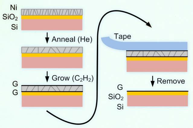
Currently, most methods of making graphene first grow the material on a film of metal, such as nickel or copper, says Hart, the Mitsui Career Development Associate Professor of Mechanical Engineering. “To make it useful, you have to get it off the metal and onto a substrate, such as a silicon wafer or a polymer sheet, or something larger like a sheet of glass,” he says. “But the process of transferring it has become much more frustrating than the process of growing the graphene itself, and can damage and contaminate the graphene.”
The new work, Hart says, still uses a metal film as the template — but instead of making graphene only on top of the metal film, it makes graphene on both the film’s top and bottom. The substrate in this case is silicon dioxide, a form of glass, with a film of nickel on top of it.
Using chemical vapor deposition (CVD) to deposit a graphene layer on top of the nickel film, Hart says, yields “not only graphene on top [of the nickel layer], but also on the bottom.” The nickel film can then be peeled away, leaving just the graphene on top of the nonmetallic substrate.
This way, there’s no need for a separate process to attach the graphene to the intended substrate — whether it’s a large plate of glass for a display screen, or a thin, flexible material that could be used as the basis for a lightweight, portable solar cell, for example. “You do the CVD on the substrate, and, using our method, the graphene stays behind on the substrate,” Hart says.
In addition to the researchers at Michigan, where Hart previously taught, the work was done in collaboration with a large glass manufacturer, Guardian Industries. “To meet their manufacturing needs, it must be very scalable,” Hart says. The company currently uses a float process, where glass moves along at a speed of several meters per minute in facilities that produce hundreds of tons of glass every day. “We were inspired by the need to develop a scalable manufacturing process that could produce graphene directly on a glass substrate,” Hart says.
The work is still in an early stage; Hart cautions that “we still need to improve the uniformity and the quality of the graphene to make it useful.” But the potential is great, he suggests: “The ability to produce graphene directly on nonmetal substrates could be used for large-format displays and touch screens, and for ‘smart’ windows that have integrated devices like heaters and sensors.”
Hart adds that the approach could also be used for small-scale applications, such as integrated circuits on silicon wafers, if graphene can be synthesized at lower temperatures than were used in the present study.
“This new process is based on an understanding of graphene growth in concert with the mechanics of the nickel film,” he says. “We’ve shown this mechanism can work. Now it’s a matter of improving the attributes needed to produce a high-performance graphene coating.”
Christos Dimitrakopoulos, a professor of chemical engineering at the University of Massachusetts at Amherst who was not involved in this work, says, “This is a very significant piece of work for very large-area applications of graphene on insulating substrates.” Compared to other methods, such as the use of a silicon carbide (SiC) substrate to grow graphene, he says, “The fact that the lateral size of graphene in the Hart group’s approach is limited only by the size of the [CVD] reactor, instead of the size of the SiC wafer, is a major advantage.”
“This is a high-quality and carefully executed work,” Dimitrakopoulos adds.
The work was supported by Guardian Industries, the National Science Foundation, and the Air Force Office of Scientific Research.
Controlling the mobility of water molecules is of relevance to several scientific disciplines and has implications in multiple technological applications.
For instance, water adsorption/desorption in nanoporous materials, such as zeolites, has potential in long-term thermal storage and energy engineering9, 10; filters with nanopores and nanochannels are increasingly explored for their large surface area and higher efficiency11, 12; in heat transfer problems, nanofluids are under investigation because of their peculiar thermal properties13, 14; in micro/nanotechnology processes, controlling the deposition and surface diffusion of water molecules is critical for precise manufacturing15, 16; in biology, the mechanisms regulating the transport of single water molecules through cell membrane channels (aquaporins) and the multi-scale water compartmentalization in tissues are still elusive17, 18, 19, 20. Also, proteins tend to modify their structure and function according to the surrounding aqueous environment21, 22.
Certainly, nanomedicine is one of the fields where several exciting discoveries and technological applications can be directly related to the anomalous behaviour of water in confined geometries. A few examples are the enhancement in longitudinal relaxivity associated with the entrapment of Gd3+-ion complexes in mesoporous structures23, 24; the dynamics of water molecules in nanotubes and nanochannels for controlled drug delivery25, 26; and the design of hydrogel-based nano/microparticles27, 28.
In particular, the dynamics of water molecules is essential in magnetic resonance imaging (MRI), in that contrast enhancement is influenced by the local diffusion of water molecules29, 30. It is known that for paramagnetic metal complexes, such as Gd3+ ions, the Solomon–Bloembergen–Morgan theory31 would predict a change in longitudinal relaxivity r1 of the complex following a variation in the relative translational diffusion time (τD) of the water molecules surrounding the complex, and in the residence lifetime (τM) of the water molecules bound to the complex. Similarly, for magnetic nanoparticles (NPs), such as the iron oxide NPs, an increase in τD (that is, decrease in D) would enhance the transversal relaxivity r2 (ref. 32).
Hence, the modulation and precise control of the diffusion of the water molecules in the vicinity of an MRI contrast agent plays an important role in imaging performance. This concept has been already successfully proved by experiments23, but a clear rationale (and a computationally efficient tool) for optimally designing such agents is still missing.
Despite its fundamental importance in science and technology, the physical and transport properties of water are far from being completely understood1. The self-diffusion of water molecules D in proximity of solid surfaces, at the interface between immiscible liquids, and in confined geometries, such as nanopores and nanotubes, is a very different process as compared to the bulk phase2, 3, 4.
The thermal agitation of the water molecules in the bulk liquid is only dictated by the local temperature and pressure conditions, and molecular diffusion follows the Einstein relation5. Differently, under confined conditions, the mobility of water molecules is perturbed by the presence of additional interaction forces arising at the water/solid interfaces, mainly van der Waals and Coulomb interactions. These additional forces usually reduce the local molecular diffusion6, 7. Even if considerable work has been done in recent years, both experimentally and theoretically, to understand and characterize the perturbed behaviour of the water molecules in confined geometries, there is still no complete comprehension of the process and often the published results are contradictory8.
In this work, the self-diffusion coefficient D of water molecules is investigated through molecular dynamics (MD) simulations under five different isothermal configurations, namely, within silica (SiO2) nanopores, around spherical hydroxylated NPs, within SiO2 nanopores filled by NPs, around single-wall carbon nanotubes (CNTs) and proteins. The coefficient D has been estimated for almost 60 cases by varying the size of the NPs and nanopores, the electrostatic surface charges and level of hydrophobicity, as well as the type of protein. The self-diffusion coefficient D for all different configurations has been found to scale with a single non-dimensional parameter θ, incorporating both geometrical and physicochemical information, following the relationship D(θ)=DB[1+(DC/DB−1)θ]. The D(θ) scaling is modulated by the coefficients DB and DC, which represent the bulk and totally confined diffusion of water, respectively. This D(θ) law has been applied to estimate the enhancement in MRI contrast in magnetic nanoconstructs obtained by geometrically confining super-paramagnetic iron oxide NPs (SPIOs) into silicon mesoporous matrices. It has been confirmed that the transversal relaxivity of SPIOs can be significantly augmented by modulating the diffusion of water molecules. This law would help in explaining and rationalizing previous experimental evidences23, and represent a ready-to-use tool for the rational design of nanoconstructs based on the nanoscale confinement of water molecules.
Computing the diffusion of nanoconfined water molecules
MD simulations were used to compute the self-diffusion coefficient D of water molecules confined under different configurations. These are shown in Fig. 1 and include the case of water molecules (blue dots) moving (a) around spherical hydroxylated nanoparticles (NPs) (grey dots); (b) within a hydrated nanopore (grey dots); (c) around hydroxylated NPs (red dots) adsorbed on the surface of a hydrated nanopore (grey dots); (d) around and within single-walled carbon nanotubes (CNTs); (e,f) around proteins. The NPs are made out of magnetite (Fe3O4) crystals (red and cyan dots), with OH− functional groups on their surface, or SiO2 crystals (grey dots), with silanol SiOH functional groups on the surface. The nanopores are made out of SiO2 only.
Figure 1: Selected configurations.
(a) SiO2 particle in water, diameter φ=5.2 nm (blue dots: water molecules; grey dots: SiO2 atoms); (b) SiO2 nanopore filled by water, diameter Φ=8.1 nm; (c) sixteen Fe3O4 NPs within a SiO2 nanopore filled by water, φ=2.0 nm and Φ=8.1 nm (red and cyan dots: Fe3O4 atoms); (d) single-walled CNT with chirality (5,5); (e) green fluorescence protein; (f) leptin protein (the standard ribbon visualization of secondary structures has been used for proteins). In d–fwater molecules have been removed for clarity. Almost 60 different cases have been analysed by varying the size and surface properties of the NPs, nanopores and nanotubes as well as the type of protein.
To Read the Full Text and Results Go to This Link:
This work is licensed under a Creative Commons Attribution 3.0 Unported License. The images or other third party material in this article are included in the article’s Creative Commons license, unless indicated otherwise in the credit line; if the material is not included under the Creative Commons license, users will need to obtain permission from the license holder to reproduce the material. To view a copy of this license, visit http://creativecommons.org/licenses/by/3.0/
A new breakthrough in nanotechnology has expanded the idea of wearable electronics. Ultra-thin and flexible electronics made entirely from carbon-based materials could be applied to essentially any surface, including plants, insects, fabric, paper, even our fingernails. These tiny electronics could be transistors, electrodes, interconnects, and, most promising, sensors.
Developed by researchers at Ulsan National Institute of Science and Technology (UNIST) in Ulsan Metropolitan City, South Korea, and the Korea Electrotechnology Research Institute in Changwon, South Korea, this new type of electronics could be easily mass produced and used to detect airborne toxins and pollutants, environmental data like humidity and temperature, and human health conditions like infections and diabetes.
Phys.org reports, “The new approach takes advantage of the unique atomic geometries of carbon to synthesize entire arrays of electronic devices, specifically carbon nanotube transistors, carbon nanotube sensors, and graphite electrodes.”
The electronics are made with antennas integrated in them, so wireless transmissions of power and sensing signals are possible without an onboard battery. The electronics can be applied to various surfaces by simply wetting them first. So far researchers have applied them to bamboo leaves, stag beetles, fingernails, particulate masks, protective arm sleeves, newspaper and adhesive tape.
They were able to use the sensors to successfully detect DMMP vapor, which is used in nerve agents like soma and sarin gas.
“In this paper, we just demonstrated the detection of the nerve gas using the biocompatible devices,” coauthor Jang-Ung Park, Assistant Professor at UNIST, told Phys.org. “As our future research, we will develop various sensing systems, including diabetes, pollutions and radioactivity, using the wearable electronic devices.”
Nerve agents are among the world’s most feared chemical weapons, but scientists at the National Institute of Standards and Technology (NIST) have demonstrated a way to engineer carbon nanotubes to dismantle the molecules of a major class of these chemicals.* In principle, they say, the nanotubes could be woven into clothing that destroys the nerve agents on contact before they reach the skin.
Single-walled carbon nanotubes, represented by the gray cylinders, can be combined with a catalyst (purple ribbons) that is capable of breaking down Sarin and related toxins into less dangerous components. The idea might one day be used to create clothing for increased protection against nerve agents.
Credit: NIST
The team’s experiments show that nanotubes—special molecules that resemble cylinders formed of chicken wire—can be combined with a copper-based catalyst able to break apart a key chemical bond in the class of nerve agents that includes Sarin.
A small amount of catalyst can break this bond in a large number of molecules, potentially rendering a nerve agent far less harmful. Because nanotubes further enhance the breakdown capability of the catalyst and can be woven into fabric easily, the NIST team members say the findings could help protect military personnel involved in cleanup operations.
Sarin—used in a 1995 Tokyo subway attack—is one of several deadly nerve agents of a group called organophosphates. Many are classified as weapons of mass destruction. While organophosphates are harmful if inhaled, they also are dangerous if absorbed through the skin, and can be even be re-released from clothing if not thoroughly decontaminated.
To protect themselves during research, the team did not work with actual nerve agents, but instead used a “mimic molecule” that contains a chemical bond identical to the one found in organophosphates. Breaking this bond splits the molecule into pieces that are far less dangerous.
The team developed a way to attach the catalyst molecule to the nanotubes and then tested the effectiveness of the tube-catalyst complex to break the bonds. To perform the test, the complex was deposited onto a small sheet of paper and put into a solution containing the mimic molecule. For comparison, the catalyst without nanotubes was tested simultaneously in a different solution. Then it was a simple matter of stirring and watching chemistry in action.
“The solution was initially transparent, almost like water,” says the team’s John Heddleston, “but as soon as we added the paper, the solution started to turn yellow as the breakdown product accumulated. Measuring this color change over time told us the amount and rate of catalysis. We began to see a noticeable difference within an hour, and the longer we left it, the more yellow it became.” The catalyst-nanotube complex far outperformed the catalyst alone.
Principal investigator Angela Hight Walker says that several questions will need to be addressed before catalytic nanotubes start showing up in clothing, such as whether it is better to add the catalyst to the nanotubes before or after they are woven into the fabric.
“We’d also like to find ways to make the catalytic reaction go faster, which is always better,” Hight Walker says. “But our research group has been focusing on the fundamental science of nanoparticles for years, so we are in a good position to answer these questions.”
*M.M. Bailey, J.M. Heddleston, J. Davis, J.L. Staymates and A.R. Hight Walker. Functionalized, carbon nanotube material for the catalytic degradation of organophosphate nerve agents. Nano Research, DOI:10.1007/s12274-014-0405-3, Nano Research 2014, 7(3): 390–398.
It has been shown before (here, and here for example) that graphene can make excellent highly sensitive strain sensors. One of the applications is human health evaluation via physiological motion detection and now researchers from two universities in China developed a method that uses graphene based sensors to monitor human motions.
The researchers developed simple-structured and low-cost graphene woven fabrics (GWFs) strain sensor. The GWFs were made using CVD to grow graphene on crisscross copper meshes. The copper mash was later etched away and the graphene fabric was transferred to a pretreated film composited with medical tape and PDMS glue, which is a flexible, biocompatible, shape controllable material. Silver wires were used to connect the graphene.
When used as a human motion sensor, the signals of GWFs resistance change depend on deformation strain which is formed by the motions. The stronger the motion is, the larger the strain is, and the easier the motion signals can be recorded.
Researchers find a two-dimensional, self-assembling material that might produce solar cells or transistors.
David L. Chandler | MIT News Office
April 30, 2014
Researchers around the world have been working to harness the unusual properties of graphene, a two-dimensional sheet of carbon atoms. But graphene lacks one important characteristic that would make it even more useful: a property called a bandgap, which is essential for making devices such as computer chips and solar cells.
Now, researchers at MIT and Harvard University have found a two-dimensional material whose properties are very similar to graphene, but with some distinct advantages — including the fact that this material naturally has a usable bandgap.
The research, just published online in the Journal of the American Chemical Society, was carried out by MIT assistant professor of chemistry Mircea Dincă and seven co-authors.
The new material, a combination of nickel and an organic compound called HITP, also has the advantage of self-assembly: Its constituents naturally assemble themselves, a “bottom-up” approach that could lend itself to easier manufacturing and tuning of desired properties by adjusting relative amounts of the ingredients.
Research on such two-dimensional materials, which often possess extraordinary properties, is “all the rage these days, and for good reason,” Dincă says. Graphene, for example, has extremely good electrical and thermal conductivity, as well as great strength. But its lack of a bandgap forces researchers to modify it for certain uses — such as by adding other molecules that attach themselves to its structure — measures that tend to degrade the properties that made the material desirable in the first place.
The new compound, Ni3(HITP)2, shares graphene’s perfectly hexagonal honeycomb structure. What’s more, multiple layers of the material naturally form perfectly aligned stacks, with the openings at the centers of the hexagons all of precisely the same size, about 2 nanometers (billionths of a meter) across.
In these initial experiments, the researchers studied the material in bulk form, rather than as flat sheets; Dincă says that makes the current results — including excellent electrical conductivity — even more impressive, since these properties should be better yet in a 2-D version of the material. “There’s every reason to believe that the properties of the particles are worse than those of a sheet,” he says, “but they’re still impressive.”
What’s more, this is just the first of what could be a diverse family of similar materials built from different metals or organic compounds. “Now we have an entire arsenal of organic synthesis and inorganic synthesis,” Dincă says, that could be harnessed to “tune the properties, with atom-like precision and virtually infinite tunability.”
Such materials, Dincă says, might ultimately lend themselves to solar cells whose ability to capture different wavelengths of light could be matched to the solar spectrum, or to improved supercapacitors, which can store electrical energy until it’s needed.
In addition, the new material could lend itself to use in basic research on the properties of matter, or to the creation of exotic materials such as magnetic topological insulators, or materials that exhibit quantum Hall effects. “They’re in the same class of materials that have been predicted to have exotic new electronic states,” Dincă says. “These would be the first examples of these effects in materials made out of organic molecules. People are excited about that.”
Pingyun Feng, a professor of chemistry at the University of California at Riverside who was not involved in this work, says the approach used by this team is “novel and surprising,” and that “the quality of this work, from the synthetic design strategy to the probing of the structural details and to the discovery of exceptional electrical conductivity, is outstanding.” She adds that this finding “represents a major advance in the synthetic design of novel semiconducting materials.”
The work was supported by the U.S. Department of Energy and the Center for Excitonics at MIT.
The courtyard between MIT.nano and Building 4 looking west from Building 8 toward the Great Dome. Image: Wilson Architects
Starting in 2018, researchers from across MIT will be able to take advantage of comprehensive facilities for nanoscale research in a new building to be constructed at the very heart of the Cambridge campus.
The 200,000-square-foot building, called “MIT.nano,” will house state-of-the-art cleanroom, imaging, and prototyping facilities supporting research with nanoscale materials and processes—in fields including energy, health, life sciences, quantum sciences, electronics, and manufacturing. An estimated 2,000 MIT researchers may ultimately make use of the building, says electrical engineering professor Vladimir Bulović, faculty lead on the MIT.nano project and associate dean for innovation in the School of Engineering.
“MIT.nano will sit at the heart of our campus, and it will be central to fulfilling MIT’s mission in research, education, and impact,” says MIT President L. Rafael Reif. “The capabilities it provides and the interdisciplinary community it inspires will keep MIT at the forefront of discovery and innovation, and give us the power to solve urgent global challenges. By following the lead of faculty and student interest, MIT has a long tradition of placing bold bets on strategic future technologies, and we expect MIT.nano to pay off in the same way, for MIT and for the world.”
MIT.nano will house two interconnected floors of cleanroom laboratories containing fabrication spaces and materials growth laboratories, greatly expanding the Institute’s capacity for research involving components that are measured in billionths of a meter—a scale at which cleanliness is paramount, as even a single speck of dust vastly exceeds the nanoscale. The building will also include the “quietest” space on campus—a floor optimized for low vibration and minimal electromagnetic interference, dedicated to advanced imaging technologies—and a floor of teaching laboratory space. Finally, the facility will feature an innovative teaching and research space, known as a Computer-Aided Visualization Environment (CAVE), allowing high-resolution views of nanoscale features.
“The tools of nanotechnology will play a critical part in how many engineering disciplines solve the problems of the 21st century, and MIT.nano will shape the Institute’s role in these advances,” says Ian A. Waitz, dean of the School of Engineering and the Jerome C. Hunsaker Professor of Aeronautics and Astronautics. “This project represents one of the largest commitments to research in MIT’s history. MIT.nano will carry the last two decades of research into new realms of application and discovery.”
“Usually we talk about how science enables new technology, but discovery is a two-way street,” adds Maria Zuber, MIT’s vice president for research and the E.A. Griswold Professor of Geophysics. “In MIT.nano, technology will advance basic science through the extraordinary observations that will be possible in this state-of-the-art facility.”
MIT.nano will be a 200,000-square-foot research facility for nanoscale research constructed at the very heart of the MIT campus. The building will house state-of-the-art cleanroom, imaging, and prototyping facilities supporting research with nanoscale materials and processes—in fields including energy, health, life sciences, quantum sciences, electronics, and manufacturing.
The four-level MIT.nano will replace the existing Building 12, and will retain its number, occupying a space alongside the iconic Great Dome. It will be interconnected with neighboring buildings, and accessible from MIT’s Infinite Corridor—meaning, Bulović says, that the new facility will be just a short walk from the numerous departments that will use its tools.
“This building needs to be centrally located, because nanoscale research is now central to so many disciplines,” says Bulović, who is the Fariborz Maseeh Professor in Emerging Technology at MIT.
Users of the new facility, he adds, are expected to come from more than 150 research groups at MIT. They will include, for example, scientists who are working on methods to “print” parts of human organs for transplantation; who are creating superhydrophobic surfaces to boost power-plant efficiency; who work with nanofluids to design new means of locomotion for machines, or new methods for purifying water; who aim to transform the manufacturing of pharmaceuticals; and who are using nanotechnology to reduce the carbon footprint of concrete, the world’s most ubiquitous building material.
The research that will take place in MIT.nano could also help the world meet its growing energy needs, Bulović says. For example, cloud computing already consumes 1.3% of the world’s electricity; as this technology proliferates, its energy use is projected to grow a thousandfold over the coming decade. Hardware based on nanoscale switching elements—a new technology now being pursued by MIT researchers—could prove crucial in reducing the energy footprint of cloud computing.
“But we have many urgent challenges that existing technology cannot address,” Bulović says. “If we want to make sweeping change—more than incremental progress—in the most urgent technical areas, we need this building and the tools of nanoscience and nanotechnology housed within it.”
“The need for advanced facilities to support nanoscale research was identified in 2011 as the Institute’s highest academic priority as part of the MIT 2030 process to envision how our campus might evolve to meet future needs for research and education,” says Israel Ruiz, MIT’s executive vice president and treasurer. “It is wonderful to see we are boldly moving to accomplish our goal.”
Cleanroom facilities, by their nature, are among the most energy-intensive buildings to operate: Enormous air-handling machinery is needed to keep their air filtered to an extraordinarily high standard. Travis Wanat, the senior project manager at MIT who is overseeing the MIT.nano project, explains that while ventilation systems for ordinary offices or classrooms are designed to exchange the air two to six times per hour, cleanroom ventilation typically requires a full exchange 250 times an hour. The fans and filters necessary to handle this volume of air require an entire dedicated floor above each floor of cleanrooms in MIT.nano.
But MIT.nano will incorporate many energy-saving features: Richard Amster, director of campus engineering and construction, has partnered with Julie Newman, MIT’s director of sustainability. Together, they are working within MIT, as well as with the design and contracting teams, “to develop the most efficient building possible for cleanroom research and imaging,” Amster says.
Toward that end, MIT.nano will use heat-recovery systems on the building’s exhaust vents. The building will also be able to sense the local cleanroom environment and adjust the need for air exchange, dramatically reducing MIT.nano’s energy consumption. Dozens of other features aim to improve the building’s efficiency and sustainability.
Despite MIT.nano’s central location, the floor devoted to advanced imaging technology will have “more quiet space than anywhere on campus,” Bulović says: The facility is situated as far as possible from the noise of city streets and subway and train lines that flank MIT’s campus.
Indeed, protection from these sources of noise and mechanical vibration dictated the building’s location, from among five campus sites that were considered. According to national standards on ambient vibration, Bulović says, parts of MIT.nano will rate two levels better than the standard typically used for such high-quality imaging spaces.
Another important goal of the building’s design—by Wilson Architects in Boston—is the creation of environments that foster interactions among users, including those from different disciplines. The building’s location at a major campus “crossroads,” its extensive use of glass walls that allow views into lab and cleanroom areas, and its soaring lobbies and other common areas are all intended to help foster such interactions.
“Nanoscale research is inherently interdisciplinary, and this building was designed to encourage collaboration,” Bulović says.
“MIT’s enduring leadership in technology and science is made possible by the interconnective nature of our community, and our total potential is greater than the sum of our parts,” adds Timothy Swager, the John D. MacArthur Professor of Chemistry. “At an intellectual level this is driven by our collective commitment to excellence and innovation, but the physical proximity of researchers at MIT is the heart and soul of this special atmosphere. MIT.nano will serve to enhance these interactions and provide an opportunity-rich venue where chemistry, biology, physics, and engineering all converge to create devices and understanding that will empower MIT researchers to reach new heights in innovation.”
The choice of MIT.nano’s central location is not without compromise, Bulović says: There is very limited access to the construction site—only three access roads, each with limited headroom—so planning for the activities of construction and delivery vehicles, and for the demolition of the current Building 12 and construction of MIT.nano, will present a host of logistical challenges. “It’s like building a ship in a bottle,” Bulović says.
But addressing those challenges will ultimately be well worth it, he says, pointing out that an estimated one-quarter of MIT’s graduate students and 20 percent of its researchers will make use of the facility. The new building “signifies the centrality of nanotechnology and nanomanufacturing for the needs of the 21st century. It will be a key innovation hub for the campus.”
All current occupants of Building 12 will be relocated by June, when underground facilities work, to enable building construction, will commence; at that point, fences will be erected around the constriction zone. The existing Building 12 will be demolished in spring 2015 and construction of MIT.nano is slated to begin in summer 2015.


 From solar panels to batteries, algorithms are becoming key to designing new materials


 ©
© 


You must be logged in to post a comment.