 (Nanowerk Spotlight) Semiconductor fabs are large, complex industrial sites with costs for a single facility approaching $10B. In this article we discuss the possibility of putting the entire functionality of such a fab onto a single silicon chip.
We demonstrate a path forward where, for certain applications, especially at the nanometer scale, one might consider using a single chip approach for building devices, both integrated circuits and nano-electromechanical systems. Such methods could mean shorter device development and fabrication times with a significant potential for cost savings. In our approach, we build micro versions of the macro machines one typically finds in a fab, allowing for the functionality to be placed on a single silicon substrate. We argue that the technology will soon exist to allow one to build a “Fab on a Chip”.
Moore’s Law is a well-known concept. According to the observation first made by Gordon E. Moore, Intel’s then CEO, the number of transistors on an IC doubles roughly every two years1. Less well known is Rock’s Law, sometimes called Moore’s Second Law, which says that semiconductor fabrication facilities, or fabs, double in cost roughly every four years2.
Current typical costs for a state-of-the-art fab range from $3-4B and can even reach up to ~$9.3B for TSMC’s recent 300mm fab in Taiwan3. Eventually Rock’s Law must run into Herbert Steins’ observation that “If something cannot go on forever, it will stop”. What can or will happen to semiconductor fabs before their costs exceed the GDP of the planet? A standard answer among nanotechnology researchers is that chemically or biologically inspired “bottom-up” approaches will be developed that will allow us to grow very-large-scale integration (VLSI) circuits in the same way we currently grow carbon nanotubes4, tomatoes or chickens.
Here, the question we pose is whether another approach to solving this problem is feasible. Would it be possible to place the entire functionality of a semiconductor fab on a single silicon chip? In the same way as we can contemplate building a “Lab on a Chip”, can we build a “Fab on a Chip” (FoC)?
For the impatient among you, we will argue here that the answer is likely to be a qualified “yes”. As semiconductor technologies continue to shrink from the deep sub-micron regime into the nanometer regime, standard techniques to manufacture the devices are becoming more and more challenging. The conventional methods using photo resist, liftoff and optical/deep-UV/E-beam lithography5, 6 have created the need for multi-billion dollar fabs, but they have no hope of ultimately scaling into the regime of single or few atom devices.
However, it is clear that progress in device physics is advancing such that in the not too distant future, we will need and desire single atom devices7 despite the fact that we have no clear idea of how such circuits could be made using a manufacturable process.

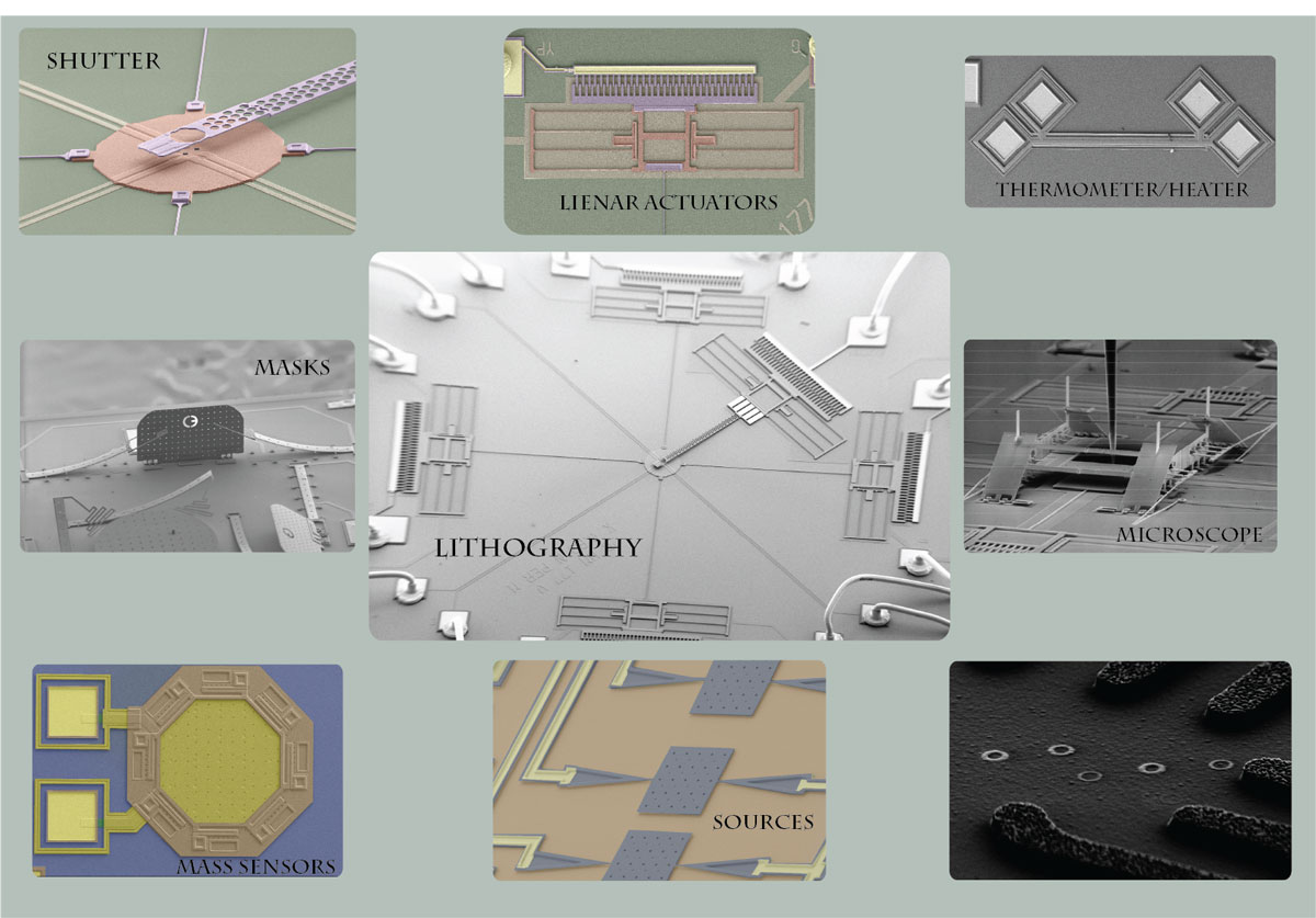
Scanning electron micrographs of MEMS devices that may be included in a FoC. Clockwise from the top: Linear Actuators and springs provide nanoscale position control, thermometers and heaters control the surface temperature. A MEMS controlled near-field scanning optical microscope can image in situ deposited structures. Thermal sources provide an atom flux that is detected by mass sensors for controlled deposition rates. Masks and dynamic shutters guide the atom flux with both high special and temporal accuracy‡. (Figures are compiled from the work of J. Chang, B. Corman, K. Frink, H. Han, M. Imboden, and references [11,21]). (click image to enlarge)
Our suggested approach is to build MEMS micro versions of the various systems one finds in a semiconductor fab. These various elements can then be placed on a silicon die allowing one to build devices with nano-scale features. What does a fab actually do? At the meta level it takes silicon wafers and grows arrays of transistors upon them with the appropriate electrical interconnects. Could a “Fab on a Chip” do this? Yes, it could. Is a “Fab on a Chip” ever going to build a 10 cm2 square silicon VLSI die with 1010 CMOS transistors on it?
Probably not, but one could imagine using a “Fab on a Chip” to build a square mm device with 108 nano-scale single electron transistors on it with the appropriate interconnects. If this later type of device is of interest to you, a “Fab on a Chip” might be just the thing.
Where between these two limits the FoC technology will run out of gas is currently an open but interesting question. A key feature to FoC technology is that one will not use photoresist and liftoff techniques. This is an enormous simplification in terms of reducing the complexity of the traditional fab. For a FoC, the deposition step uses a direct write approach8-12.
There are a number of possible methods. One such a device is shown in the figure. It is a MEMS plate with an integrated shutter allowing for the direct writing of atoms, analogous to a micro 3-D printer11, 13. This (or something like it) would be the lithography tool with nanoscale displacement resolution. In addition to the lithography tool, one needs sources of atoms (thermally sourced from micro-heaters14 or ions from micro-spray emitters15), film thickness monitors based on mechanical oscillators for controlled deposition16-18, resistive heaters9,19, thermometers20, shutters/masks, imaging tools21 and electrical interconnects that all work together to monitor and control the fabrication environment and possibly even including an integrated power source22.
Examples of such MEMS elements are also shown in the figure. All the devices can be placed onto a single silicon die and together, could be used to create a nano-scale system of devices. The devices shown in the figure were built using a commercial foundry and can be easily arrayed on a single silicon die23, resulting in a so-called “system of systems” approach.
Many questions abound such as: Would such chips be cost effective? High yield? Reliable? Low Waste? Are we insane to suggest this? At the moment the answer these and many other similar questions is “maybe”.
In a very real sense, what we are suggesting is using macro-machines to build micro-machines and then using these micro-machines to build nanostructure elements of electrical circuits and nano-electromechanical systems. The concept of producing micron-scale MEMS devices (which cost roughly a dollar per square mm to produce, and perhaps even a factor of ten less in large volumes) and then using nanometer tunability to create nano-scale devices opens up a new and perhaps much less expensive avenue towards manufacturing large arrays of nano-scale devices.
We believe it is fair to call this approach a “Fab on a Chip” because in addition to the lithography piece, one can integrate onto the silicon chip many of the other functions a semiconductor fab performs and at the end of the day, these chips would produce what fabs produce: a silicon die with arrays of devices on them.
Will such an approach be a “holy grail” that solves all the problems associated with producing nano-scale VLSI circuits? Probably not. Will it allow us to produce certain types of nano-scale circuits in a cost effective way? We believe so. Is it an interesting and potentially important avenue to research? Absolutely.
Notes 1. Moore, G. The Future of Integrated Electronics. Fairchild Semiconductor internal publication (1964). 2. Rupp, K. & Selberherr, S. The economic limit to Moore’s law. Semiconductor Manufacturing, IEEE Transactions on 24, 1-4 (2011). 3. TSMC Begins Construction on Gigafab™ In Central Taiwan 4. Li, X., Cao, A., Jung, Y. J., Vajtai, R. & Ajayan, P. M. Bottom-up growth of carbon nanotube multilayers: unprecedented growth. Nano Letters 5, 1997-2000 (2005). 5. Ito, T. & Okazaki, S. Pushing the limits of lithography. Nature 406, 1027-1031 (2000). 6. Grigorescu, A. & Hagen, C. Resists for sub-20-nm electron beam lithography with a focus on HSQ: state of the art. Nanotechnology 20, 292001 (2009). 7. Rossier, J. F. Single-atom devices: Quantum engineering. Nature Materials 12, 480-481 (2013). 8. Lee, W., et al. Direct-write polymer nanolithography in ultra-high vacuum. Beilstein Journal of Nanotechnology 3, 52-56 (2012). 9. Savu, V., Xie, S. & Brugger, J. 100 mm dynamic stencils pattern sub-micrometre structures. Nanoscale 3, 2739-2742 (2011). 10. Meister, A., Liley, M., Brugger, J., Pugin, R. & Heinzelmann, H. Nanodispenser for attoliter volume deposition using atomic force microscopy probes modified by focused-ion-beam milling. Appl.Phys.Lett. 85, 6260-6262 (2004). 11. Imboden, M., et al. Atomic Calligraphy: The Direct Writing of Nanoscale Structures using MEMS. Nano Letters (2013). Also see Nanowerk Spotlight: “Atomic calligraphy – using MEMS to write nanoscale structures”. 12. Tseng, A. A. Advancements and challenges in development of atomic force microscopy for nanofabrication. Nano Today 6, 493-509 (2011). 13. Egger, S., et al. Dynamic shadow mask technique: A universal tool for nanoscience. Nano Letters 5, 15-20 (2005). 14. Darhuber, A. A., Valentino, J. P., Troian, S. M. & Wagner, S. Thermocapillary actuation of droplets on chemically patterned surfaces by programmable microheater arrays. Journal of Microelectromechanical Systems, 12, 873-879 (2003). 15. Krpoun, R., Smith, K. L., Stark, J. P. & Shea, H. Tailoring the hydraulic impedance of out-of-plane micromachined electrospray sources with integrated electrodes. Appl.Phys.Lett. 94, 163502-163502-3 (2009). 16. Chaste, J., et al. A nanomechanical mass sensor with yoctogram resolution. Nature Nanotechnology (2012). 17. Lang, H. P., Hegner, M. & Gerber, C. Cantilever array sensors. Materials today 8, 30-36 (2005). 18. Arcamone, J., et al. Full-wafer fabrication by nanostencil lithography of micro/nanomechanical mass sensors monolithically integrated with CMOS. Nanotechnology 19, 305302 (2008). 19. Laconte, J., Dupont, C., Flandre, D. & Raskin, J. SOI CMOS compatible low-power microheater optimization for the fabrication of smart gas sensors. Sensors Journal, IEEE 4, 670-680 (2004). 20. Jha, C., et al. CMOS-compatible dual-resonator MEMS temperature sensor with milli-degree accuracy. Solid-State Sensors, Actuators and Microsystems Conference, 2007. TRANSDUCERS 2007. 229-232 (2007). 21. Aksyuk, V. A., Barber, B. P., Gammel, P. L. & Bishop, D. J. Construction of a fully functional NSOM using MUMPs technology. Proceedings Volume 3226: Microelectronic Structures and MEMS for Optical Processing III, 188-194 (1997). 22. Pikul, J. H., Zhang, H. G., Cho, J., Braun, P. V. & King, W. P. High-power lithium ion microbatteries from interdigitated three-dimensional bicontinuous nanoporous electrodes.
Nature Communications 4, 1732 (2013). 23.
http://www.memscap.com/products/mumps/polymumps/reference-material By Matthias Imboden and David Bishop, Department of Electrical and Computer Engineering, Division of Materials Science and Engineering, Department of Physics, Boston University
Read more: http://www.nanowerk.com/spotlight/spotid=31758.php#ixzz2buaHWFKT


You must be logged in to post a comment.