New Carbon Capture Hybrid-Membrane Boasts Greenhouse Gas Reductions


GH Gas 031716 global-climate-change

Hybrid materials developed at Berkeley Lab could lead to cheaper ways to reduce power plant greenhouse gas emissions

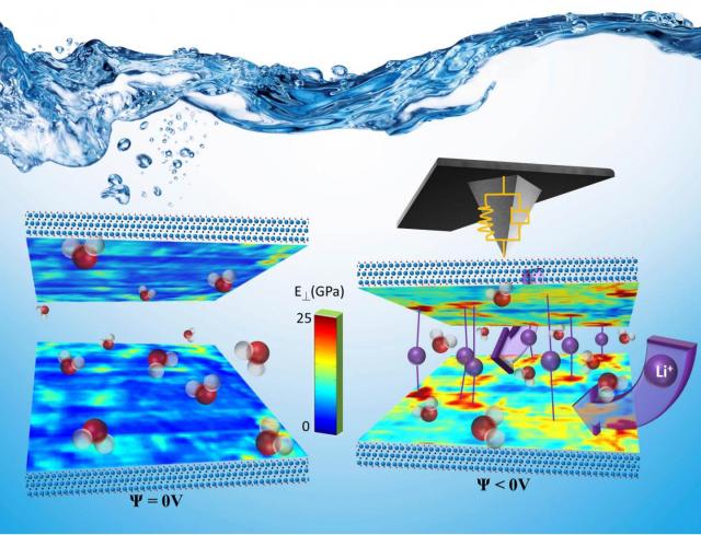
In this animation, exhaust from a power plant contacts a hybrid membrane recently developed at Berkeley Lab. The membrane’s carbon dioxide highways (yellow) enable the rapid flow of carbon dioxide (red and white molecules) while maintaining selectivity over nitrogen (blue molecules). The membrane is eight times more carbon dioxide permeable than a polymer-only membrane. (Credit: Berkeley Lab)

A new, highly permeable carbon capture membrane developed by scientists from the U.S. Department of Energy’s Lawrence Berkeley National Laboratory (Berkeley Lab) could lead to more efficient ways of separating carbon dioxide from power plant exhaust, preventing the greenhouse gas from entering the atmosphere and contributing to climate change.

The researchers focused on a hybrid membrane that is part polymer and part metal-organic framework, which is a porous three-dimensional crystal with a large internal surface area that can absorb enormous quantities of molecules.

In a first, the scientists engineered the membrane so that carbon dioxide molecules can travel through it via two distinct channels. Molecules can travel through the polymer component of the membrane, like they do in conventional gas-separation membranes. Or molecules can flow through “carbon dioxide highways” created by adjacent metal-organic frameworks.

Initial tests show this two-route approach makes the hybrid membrane eight times more carbon dioxide permeable than membranes composed only of the polymer. Boosting carbon dioxide permeability is a big goal in efforts to develop carbon capture materials that are energy efficient and cost competitive.

The research is the cover article of the March issue of the journal Energy & Environmental Science.

“In our membrane, some CO2 molecules get an express ride through the highways formed by metal-organic frameworks, while others take the polymer pathway. This new approach will enable the design of higher performing gas separation membranes,” says Norman Su, a graduate student in the Chemical and Biomolecular Engineering Department at UC Berkeley and a user at the Molecular Foundry.

He conducted the research with Jeff Urban, Facility Director of the Inorganic Nanostructures Facility at the Molecular Foundry, and a team of scientists that included staff at the Advanced Light Source.

Capturing carbon emissions from electric power plants and other sources is a hot research topic because there’s a lot of room for improvement. The conventional way of separating carbon dioxide from flue gas is amine adsorption, which isn’t economical at scale because it adds significant capital cost and reduces the electrical output of power plants.

Scientists are exploring polymer membranes as a more energy efficient alternative to amine adsorption. These membranes are relatively inexpensive and easy to work with, but current commercial membranes have low carbon dioxide permeability. To overcome this, scientists have developed hybrid membranes that are part polymer and part metal-organic framework. These hybrids harness the carbon dioxide selectivity of metal-organic frameworks while maintaining the processability of polymers.

But, until now, scientists have not been able to engineer hybrid membranes with enough metal-organic frameworks to form continuous channels through the membrane. This means that, somewhere in a carbon dioxide molecule’s journey through the membrane, the molecule must contact the polymer. This constrains the molecule’s transport to the polymer.

In this latest research, Berkeley Lab scientists have developed a hybrid membrane in which metal-organic frameworks account for 50 percent of its weight, which is about 20 percent more than other hybrid membranes. Previously, the mechanical stability of a hybrid membrane limited the amount of metal-organic frameworks that could be packed in it.

“But we got our membrane to 50 weight percent without compromising its structural integrity,” says Su.

And 50 weight percent appears to be the magic number. At that threshold, there are so many metal organic frameworks in the membrane that they form a continuous network of highways through the membrane. When that happens, the hybrid membrane switches from having a single channel to transport carbon dioxide, in which the molecules must go through the polymer, to two channels, in which the molecules can either move through the polymer or through the metal-organic framework highways.

“This is the first hybrid polymer-MOF membrane to have these dual transport pathways, and it could be a big step toward more competitive carbon capture processes,” says Su.

In addition to fabricating the hybrid membrane at the Molecular Foundry, the scientists analyzed the material at beamline 12.2.2 of the Advanced Light Source.

The research was supported by the Department of Energy’s Office of Science, Berkeley Lab’s Laboratory-Directed Research and Development Program, and the Department of Defense.

The Advanced Light Source and the Molecular Foundry are DOE Office of Science User Facilities located at Berkeley Lab.

###

Lawrence Berkeley National Laboratory addresses the world’s most urgent scientific challenges by advancing sustainable energy, protecting human health, creating new materials, and revealing the origin and fate of the universe. Founded in 1931, Berkeley Lab’s scientific expertise has been recognized with 13 Nobel prizes. The University of California manages Berkeley Lab for the U.S. Department of Energy’s Office of Science. For more, visit www.lbl.gov.

DOE’s Office of Science is the single largest supporter of basic research in the physical sciences in the United States, and is working to address some of the most pressing challenges of our time. For more information, please visit science.energy.gov

Updated:

Advanced energy storage material gets unprecedented nanoscale analysis


Advanced Nano Scale Storage 111245_web

OAK RIDGE, Tenn., March 16, 2016 — Researchers at the Department of Energy’s Oak Ridge National Laboratory have combined advanced in-situ microscopy and theoretical calculations to uncover important clues to the properties of a promising next-generation energy storage material for supercapacitors and batteries.

ORNL’s Fluid Interface Reactions, Structures and Transport (FIRST) research team, using scanning probe microscopy made available through the Center for Nanophase Materials Sciences (CNMS) user program, have observed for the first time at the nanoscale and in a liquid environment how ions move and diffuse between layers of a two-dimensional electrode during electrochemical cycling. This migration is critical to understanding how energy is stored in the material, called MXene, and what drives its exceptional energy storage properties.

“We have developed a technique for liquid environments that allows us to track how ions enter the interlayer spaces. There is very little information on how this actually happens,” said Nina Balke, one of a team of researchers working with Drexel University’s Yury Gogotsi in the FIRST Center, a DOE Office of Science Energy Frontier Research Center.

“The energy storage properties have been characterized on a microscopic scale, but no one knows what happens in the active material on the nanoscale in terms of ion insertion and how this affects stresses and strains in the material,” Balke said.

The so-called MXene material — which acts as a two-dimensional electrode that could be fabricated with the flexibility of a sheet of paper — is based on MAX-phase ceramics, which have been studied for decades. Chemical removal of the “A” layer leaves two-dimensional flakes composed of transition metal layers — the “M” — sandwiching carbon or nitrogen layers (the “X”) in the resulting MXene, which physically resembles graphite.

These MXenes, which have exhibited very high capacitance, or ability to store electrical charge, have only recently been explored as an energy storage medium for advanced batteries.

“The interaction and charge transfer of the ion and the MXene layers is very important for its performance as an energy storage medium. The adsorption processes drive interesting phenomena that govern the mechanisms we observed through scanning probe microscopy,” said FIRST researcher Jeremy Come.

The researchers explored how the ions enter the material, how they move once inside the materials and how they interact with the active material. For example, if cations, which are positively charged, are introduced into the negatively charged MXene material, the material contracts, becoming stiffer.

That observation laid the groundwork for the scanning probe microscopy-based nanoscale characterization. The researchers measured the local changes in stiffness when ions enter the material. There is a direct correlation with the diffusion pattern of ions and the stiffness of the material.

Come noted that the ions are inserted into the electrode in a solution.

“Therefore, we need to work in liquid environment to drive the ions within the MXene material. Then we can measure the mechanical properties in-situ at different stages of charge storage, which gives us direct insight about where the ions are stored,” he said.

Until this study the technique had not been done in a liquid environment.

The processes behind ion insertion and the ionic interactions in the electrode material had been out of reach at the nanoscale until the CNMS scanning probe microscopy group’s studies. The experiments underscore the need for in-situ analysis to understand the nanoscale elastic changes in the 2D material in both dry and wet environments and the effect of ion storage on the energy storage material over time.

The researchers’ next steps are to improve the ionic diffusion paths in the material and explore different materials from the MXene family. Ultimately, the team hopes to understand the process’s fundamental mechanism and mechanical properties, which would allow tuning the energy storage as well as improving the material’s performance and lifetime.

ORNL’s FIRST research team also provided additional calculations and simulations based on density functional theory that support the experimental findings. The work was recently published in the Journal Advanced Energy Materials.

###

The research team in addition to Balke and Come and Drexel’s Gogotsi included Michael Naguib, Stephen Jesse, Sergei V. Kalinin, Paul R.C. Kent and Yu Xie, all of ORNL.

The FIRST Center is an Energy Frontier Research Center supported by the DOE Office of Science (Basic Energy Sciences). The Center for Nanophase Materials Sciences and the National Energy Research Scientific Computing Center are DOE Office of Science User Facilities.

UT-Battelle manages ORNL for the DOE’s Office of Science. The Office of Science is the single largest supporter of basic research in the physical sciences in the United States, and is working to address some of the most pressing challenges of our time. For more information, please visit http://science.energy.gov/.

Image: https://www.ornl.gov/sites/default/files/news/images/JCome_MXene.jpg

Image cutline: When a negative bias is applied to a two-dimensional MXene electrode, Li+ ions from the electrolyte migrate in the material via specific channels to the reaction sites, where the electron transfer occurs. Scanning probe microscopy at Oak Ridge National Laboratory has provided the first nanoscale, liquid environment analysis of this energy storage material.

NOTE TO EDITORS: You may read other press releases from Oak Ridge National Laboratory or learn more about the lab at http://www.ornl.gov/news. Additional information about ORNL is available at the sites below:
Twitter – http://twitter.com/ornl
RSS Feeds – http://www.ornl.gov/ornlhome/rss_feeds.shtml
Flickr – http://www.flickr.com/photos/oakridgelab
YouTube – http://www.youtube.com/user/OakRidgeNationalLab
LinkedIn – http://www.linkedin.com/companies/oak-ridge-national-laboratory
Facebook – http://www.facebook.com/Oak.Ridge.National.Laboratory

Nanotechnology: The Science of the Very .. Very Small: Video


Nano 031716 invite_powerofsmall_logo

From macrosize to microsize to nanosize: great video for those learning about the potential (and awesomeness) of nanotechnology! (See an Example of ‘Nano-Crystals’ – Quantum Dots – Below). Watch the Video below:

Quantum Dots – An Example of New Nano-Materials

A quantum dot is a semiconductor nanostructure that confines the motion of conduction band electrons, valence band holes, or excitons (bound pairs of conduction band electrons and valence band holes) in all three spatial directions.


Small quantum dots, such as colloidal semiconductor nanocrystals, can be as small as 2 to 10 nanometers, corresponding to 10 to 50 atoms in diameter and a total of 100 to 100,000 atoms within the quantum dot volume.

Self-assembled quantum dots are typically between 10 and 50 nm in size.

Quantum dots defined by lithographically patterned gate electrodes, or by etching on two-dimensional electron gases in semiconductor heterostructures can have lateral dimensions exceeding 100 nm.

At 10 nm in diameter, nearly 3 million quantum dots could be lined up end to end and fit within the width of a human thumb.

Current and future applications of QDs impact a broad range of industrial markets. These include, for example:

Biology and biomedicine

Computing and memory

Electronics and displays

Optoelectronic devices such as LEDs, lighting and lasers

Optical components in telecommunications and image sensors

Security applications such as covert identification tagging or biowarfare detection sensors.

The global market for quantum dots (QDs) was estimated to generate $121 million in revenues in 2013. This market is expected to reach about $1.1 billion in 2016 and about $3.1 billion by 2018, at a compound annual growth rate (CAGR) of 90.8% for the five-year period, 2013 to 2018.


GNT Thumbnail Alt 3 2015-page-001

Genesis Nanotechnology, Inc. ~ “Great Things from Small Things”

Watch Our YouTube Video

Follow Our ‘Top Ten’ Blog: “Great Things from Small Things”

Follow Us on Twitter: @Genesisnanotech

Follow and ‘Like’ Us on Facebook

Connect with Our Website

‘Join the Conversation’ at Our LinkedIn ‘Nano Network’ Group

Quantum Dot Forum 2016: Taking Quantum Dots From the Lab to Commercial Success


Nanosys 1 -423 1429654580386
Published on Mar 12, 2016


Jason looks at how Quantum Dot technology has progressed, initially as a research topic and then as a commercial product. He defines what commercial success looks like and outlines future market opportunities for the further success of Quantum Dots. Topics include: Quantum Dot business models, architectures and long term roadmap, regulatory environment and future market opportunities.

Nanosys CEO Jason Hartlove: Video

Graphene-Wapped Nanocrystals Power A New Fuel Cell Design


newfuelcelld 031516
A powdery mixture of graphene-wrapped magnesium nanocrystals, produced at Berkeley Lab, is stable in air. The mixture’s energy properties show promise for use in hydrogen fuel cells. Credit: Eun Seon Cho/Berkeley Lab

Hydrogen is the lightest and most plentiful element on Earth and in our universe. So it shouldn’t be a big surprise that scientists are pursuing hydrogen as a clean, carbon-free, virtually limitless energy source for cars and for a range of other uses, from portable generators to telecommunications towers—with water as the only byproduct of combustion.

While there remain scientific challenges to making -based energy sources more competitive with current automotive propulsion systems and other energy technologies, researchers at the U.S. Department of Energy’s Lawrence Berkeley National Laboratory (Berkeley Lab) have developed a new materials recipe for a battery-like cell—which surrounds hydrogen-absorbing magnesium nanocrystals with atomically thin graphene sheets—to push its performance forward in key areas.

The graphene shields the nanocrystals from oxygen and moisture and contaminants, while tiny, natural holes allow the smaller hydrogen molecules to pass through. This filtering process overcomes common problems degrading the performance of metal hydrides for .

These graphene-encapsulated magnesium crystals act as “sponges” for hydrogen, offering a very compact and safe way to take in and store hydrogen. The nanocrystals also permit faster fueling, and reduce the overall “tank” size.

“Among metal hydride-based materials for hydrogen storage for vehicle applications, our materials have good performance in terms of capacity, reversibility, kinetics and stability,” said Eun Seon Cho, a postdoctoral researcher at Berkeley Lab and lead author of a study related to the new fuel cell formula, published recently in Nature Communications.

New fuel cell design powered by graphene-wrapped nanocrystals
Thin sheets of graphene oxide (red sheets) have natural, atomic-scale defects that allow hydrogen gas molecules to pass through while blocking larger molecules such as oxygen (O2) and water (H2O). Berkeley Lab researchers encapsulated …more

In a hydrogen fuel cell-powered vehicle using these materials, known as a “metal hydride” (hydrogen bound with a metal) fuel cell, hydrogen gas pumped into a vehicle would be chemically absorbed by the magnesium nanocrystaline powder and rendered safe at low pressures.

Jeff Urban, a Berkeley Lab staff scientist and co-author, said, “This work suggests the possibility of practical hydrogen storage and use in the future. I believe that these materials represent a generally applicable approach to stabilizing reactive materials while still harnessing their unique activity—concepts that could have wide-ranging applications for batteries, catalysis, and energetic materials.”

The research, conducted at Berkeley Lab’s Molecular Foundry and Advanced Light Source, is part of a National Lab Consortium, dubbed HyMARC (Hydrogen Materials—Advanced Research Consortium) that seeks safer and more cost-effective hydrogen storage, and Urban is Berkeley Lab’s lead scientist for that effort.

The U.S. market share for all electric-drive vehicles in 2015, including full-electric, hybrids and plug-in hybrid vehicles, was 2.87 percent, which amounts to about 500,000 electric-drive vehicles out of total vehicle sales of about 17.4 million, according to statistics reported by the Electric Drive Transportation Association, a trade association promoting electric-drive vehicles.

Hydrogen-fuel-cell vehicles haven’t yet made major in-roads in vehicle sales, though several major auto manufacturers including Toyota, Honda, and General Motors, have invested in developing hydrogen fuel-cell vehicles. Indeed, Toyota released a small-production model called the Mirai, which uses compressed-hydrogen tanks, last year in the U.S.

A potential advantage for hydrogen-fuel-cell vehicles, in addition to their reduced environmental impact over standard-fuel vehicles, is the high specific energy of hydrogen, which means that can potentially take up less weight than other battery systems and fuel sources while yielding more electrical energy.

A measure of the energy storage capacity per weight of hydrogen fuel cells, known as the “gravimetric energy density,” is roughly three times that of gasoline. Urban noted that this important property, if effectively used, could extend the total vehicle range of hydrogen-based transportation, and extend the time between refueling for many other applications, too.

More R&D is needed to realize higher-capacity hydrogen storage for long-range vehicle applications that exceed the performance of existing electric-vehicle batteries, Cho said, and other applications may be better suited for hydrogen fuel cells in the short term, such as stationary power sources, forklifts and airport vehicles, portable power sources like laptop battery chargers, portable lighting, water and sewage pumps and emergency services equipment.

Cho said that a roadblock to metal hydride storage has been a relatively slow rate in taking in (absorption) and giving out (desorption) hydrogen during the cycling of the units. In fuel cells, separate chemical reactions involving hydrogen and oxygen produce a flow of electrons that are channeled as electric current, creating water as a byproduct.

The tiny size of the graphene-encapsulated nanocrystals created at Berkeley Lab, which measure only about 3-4 nanometers, or billionths of a meter across, is a key in the new fuel cell materials’ fast capture and release of hydrogen, Cho said, as they have more surface area available for reactions than the same material would at larger sizes.

Another key is protecting the magnesium from exposure to air, which would render it unusable for the fuel cell, she added.

Working at The Molecular Foundry, researchers found a simple, scalable and cost-effective “one pan” technique to mix up the graphene sheets and magnesium oxide nanocrystals in the same batch. They later studied the coated nanocrystals’ structure using X-rays at Berkeley Lab’s Advanced Light Source. The X-ray studies showed how pumped into the fuel cell mixture reacted with the magnesium nanocrystals to form a more stable molecule called magnesium hydride while locking out oxygen from reaching the magnesium.

“It is stable in air, which is important,” Cho said.

Next steps in the research will focus on using different types of catalysts—which can improve the speed and efficiency of chemical reactions—to further improve the fuel cell’s conversion of electrical current, and in studying whether different types of material can also improve the fuel cell’s overall capacity, Cho said.

Explore further: Hydrogen released to fuel cell more quickly when stored in metal nanoparticles

More information: Eun Seon Cho et al. Graphene oxide/metal nanocrystal multilaminates as the atomic limit for safe and selective hydrogen storage, Nature Communications (2016). DOI: 10.1038/ncomms10804

Inventing a Fleet – Fast Test for Nanomanufacturing (nano-materials) for Quality Control


Measurements of electrical properties of a plastic tape (yellow), taken using a specially designed microwave cavity (the white cylinder at center) and accompanying electrical circuit, change quickly and consistently in response to changes in the tape’s thickness. The setup is inspired by high-volume roll-to-roll manufacturing devices used to mass-produce nanomaterials. The changes in the tape’s thickness spell NIST in Morse code.
Credit: NIST/Nathan Orloff

Manufacturers may soon have a speedy and nondestructive way to test a wide array of materials under real-world conditions, thanks to an advance that researchers at the National Institute of Standards and Technology (NIST) have made in roll-to-roll measurements. Roll-to-roll measurements are typically optical measurements for roll-to-roll manufacturing, any method that uses conveyor belts for continuous processing of items, from tires to nanotechnology components.

In order for new materials such as carbon nanotubes and graphene to play an increasingly important role in electronic devices, high-tech composites and other applications, manufacturers will need quality-control tests to ensure that products have desired characteristics, and lack flaws. Current test procedures often require cutting, scratching or otherwise touching a product, which slows the manufacturing process and can damage or even destroy the sample being tested.

To add to existing testing non-contact methods, NIST physicists Nathan Orloff, Christian Long and Jan Obrzut measured properties of films by passing them through a specially designed metal box known as a microwave cavity. Electromagnetic waves build up inside the cavity at a specific “resonance” frequency determined by the box’s size and shape, similar to how a guitar string vibrates at a specific pitch depending on its length and tension. When an object is placed inside the cavity, the resonance frequency changes in a way that depends on the object’s size, electrical resistance and dielectric constant, a measure of an object’s ability to store energy in an electric field. The frequency change is reminiscent of how shortening or tightening a guitar string makes it resonate at a higher pitch, says Orloff.

The researchers also built an electrical circuit to measure these changes. They first tested their device by running a strip of plastic tape known as polyimide through the cavity, using a roll-to-roll setup resembling high-volume roll-to-roll manufacturing devices used to mass-produce nanomaterials. As the tape’s thickness increased and decreased–the researchers made the changes in tape thickness spell “NIST” in Morse code–the cavity’s resonant frequency changed in tandem. So did another parameter called the “quality factor,” which is the ratio of the energy stored in the cavity to the energy lost per frequency cycle. Because polyimide’s electrical properties are well known, a manufacturer could use the cavity measurements to monitor whether tape is coming off the production line at a consistent thickness–and even feeding back information from the measurements to control the thickness.

Alternatively, a manufacturer could use the new method to monitor the electrical properties of a less well-characterized material of known dimensions. Orloff and Long demonstrated this by passing 12- and 15-centimeter-long films of carbon nanotubes deposited on sheets of plastic through the cavity and measuring the films’ electrical resistance. The entire process took “less than a second,” says Orloff. He added that with industry-standard equipment, the measurements could be taken at speeds beyond 10 meters per second, more than enough for many present-day manufacturing operations.

The new method has several advantages for a thin-film manufacturer, says Orloff. One, “You can measure the entire thing, not just a small sample,” he said. Such real-time measurements could be used to tune the manufacturing process without shutting it down, or to discard a faulty batch of product before it gets out the factory door. “This method could significantly boost prospects of not making a faulty batch in the first place,” Long noted.

And because the method is nondestructive, Orloff added, “If a batch passes the test, manufacturers can sell it.”

Films of carbon nanotubes and graphene are just starting to be manufactured in bulk for potential applications such as composite airplane materials, smartphone screens and wearable electronic devices.

Orloff, Long and Obrzut submitted a patent application for this technique in December 2015.

A producer of such materials has already expressed interest in the new method, said Orloff. “They’re really excited about it.” He added that the method is not specific to nanomanufacturing, and with a properly designed cavity, could also help with quality control of many other kinds of products, including tires, pharmaceuticals and even beer.


Story Source:

The above post is reprinted from materials provided by National Institute of Standards and Technology (NIST). Note: Materials may be edited for content and length.


Journal Reference:

  1. Nathan D. Orloff, Christian J. Long, Jan Obrzut, Laurent Maillaud, Francesca Mirri, Thomas P. Kole, Robert D. McMichael, Matteo Pasquali, Stephan J. Stranick, J. Alexander Liddle. Noncontact conductivity and dielectric measurement for high throughput roll-to-roll nanomanufacturing. Scientific Reports, 2015; 5: 17019 DOI: 10.1038/srep17019

Could a Commercially Viable – Revolutionary Graphene Filter – 9X Faster – Solve the Global Water Crisis?


Monash U  031116 1-revolutionar

A new type of graphene-based filter could be the key to managing the global water crisis, a study has revealed. The new graphene filter, which has been developed by Monash University and the University of Kentucky, allows water and other liquids to be filtered nine times faster than the current leading commercial filter.

According to the World Economic Forum’s Global Risks Report, lack of access to safe, clean water is the biggest risk to society over the coming decade. Yet some of these risks could be mitigated by the development of this filter, which is so strong and stable that it can be used for extended periods in the harshest corrosive environments, and with less maintenance than other filters on the market.

The research team was led by Associate Professor Mainak Majumder from Monash University. Associate Professor Majumder said the key to making their filter was developing a viscous form of oxide that could be spread very thinly with a blade.

“This technique creates a uniform arrangement in the graphene, and that evenness gives our filter special properties,” Associate Prof Majumder said.

This technique allows the filters to be produced much faster and in larger sizes, which is critical for developing commercial applications. The graphene-based filter could be used to filter chemicals, viruses, or bacteria from a range of liquids. It could be used to purify water, dairy products or wine, or in the production of pharmaceuticals.

This is the first time that a graphene filter has been able to be produced on an industrial scale – a problem that has plagued the scientific community for years.

Research team member and PhD candidate, Abozar Akbari, said scientists had known for years that graphene filters had impressive qualities, but in the past they had been difficult and expensive to produce.

“It’s been a race to see who could develop this technology first, because until now graphene-based could only be used on a small scale in the lab,” Mr Akbari said.

Graphene is a lattice of carbon atoms so thin it’s considered to be two-dimensional. It has been hailed as a “wonder-material” because of its incredible performance characteristics and range of potential applications.

The team’s new filter can filter out anything bigger than one nanometre, which is about 100,000 times smaller than the width of a human hair.

The research has gathered interest from a number of companies in the United States and the Asia Pacific, the largest and fastest-growing markets for nano-filtration technologies.

The team’s research was supported by industry partner Ionic Industries, as well as a number of Australian Research Council grants.

Ionic Industries’ CEO, Mark Muzzin, said the next step was to get the patented graphene-based filter on the market.

“We are currently developing ways to test how the filter fares against particular contaminants that are of interest to our customers” Mr Muzzin said.

Co-author of the research and Director of the Center for Membrane Science, Professor Dibakar Bhattacharyya, from the University of Kentucky, said: “The ability to control the thickness of the filter and attain a sharper cut-off in separation, and the use of only water as the casting solvent, is a commercial breakthrough.”

Explore further: Graphene’s love affair with water

More information: Abozar Akbari et al. Large-area graphene-based nanofiltration membranes by shear alignment of discotic nematic liquid crystals of graphene oxide, Nature Communications (2016). DOI: 10.1038/ncomms10891


GNT Thumbnail Alt 3 2015-page-001

Genesis Nanotechnology, Inc. ~ “Great Things from Small Things”

Watch Our YouTube Video

Follow Our ‘Top Ten’ Blog: “Great Things from Small Things”

Follow Us on Twitter: @Genesisnanotech

Follow and ‘Like’ Us on Facebook

Connect with Our Website

‘Join the Conversation’ at Our LinkedIn ‘Nano Network’ Group


Innovative catalyst fabrication method may yield breakthrough in fuel cell development


A polybenzimidazole polymer supports the formation of gold nanoparticles with well-defined sizes on graphene.
Credit: International Institute for Carbon-Neutral Energy Research (I²CNER), Kyushu University

Research group develops new method for creating highly efficient gold nanoparticle catalysts for fuel cells

The successful future of fuel cells relies on improving the performance of the catalysts they use. Gold nanoparticles have been cited as an ideal solution, but creating a uniform, useful catalyst has proven elusive. However, a team of researchers at Kyushu University’s International Institute for Carbon-Neutral Energy Research (I2CNER) devised a method for using a new type of catalyst support.

In a potential breakthrough technology for fuel cells, a recently published article in Scientific Reports shows how wrapping a graphene support in a specially prepared polymer provides an ideal foundation for making uniform, highly active gold nanoparticle catalysts.

Fuel cells produce electricity directly from the separate oxidation of the fuel and the reduction of oxygen. The only by-product of the process is water, as fuel cells produce no greenhouse gases and are widely seen as essential for a clean-energy future.

However, the rate at which electricity can be produced in fuel cells is limited, especially by the oxygen reduction reaction (ORR), which must be catalyzed in practical applications. Although current platinum-based catalysts accelerate the reaction, their unhelpful propensity to also catalyze other reactions, and their sensitivity to poisoning by the reactants, limits their overall utility. Despite bulk gold being chemically inert, gold nanoparticles are surprisingly effective at catalyzing the oxygen reduction reaction without the drawbacks associated with their platinum counterparts.

Nevertheless, actually creating uniformly sized gold nanoparticle catalysts has proven problematic. Previous fabrication methods have produced catalysts with nanoparticle sizes that were too large or too widely distributed for practical use. Meanwhile, efforts to regulate the particle size tended to restrict the gold’s activity or make less-stable catalysts.

“Creating small, well-controlled particles meant that we needed to focus on particle nucleation and particle growth,” lead and corresponding author Tsuyohiko Fujigaya says. “By wrapping the support in the polybenzimidazole polymer we successfully developed with platinum, we created a much better support environment for the gold nanoparticles.”

The team also tested the performance of these novel catalyst structures. Their catalysts had the lowest overpotential ever reported for this type of reaction. “The overpotential is a bit like the size of the spark you need to start a fire,” coauthor Naotoshi Nakashima says. “Although we’re obviously pleased with the catalysts’ uniformity, the performance results show this really could be a leap forward for the ORR reaction and maybe fuel cells as well.”

The article “Growth and Deposition of Au Nanoclusters on Polymer-wrapped Graphene and Their Oxygen Reduction Activity” was published in Scientific Reports.


Story Source:

The above post is reprinted from materials provided by Kyushu University, I2CNER. Note: Materials may be edited for content and length.


Journal Reference:

  1. Tsuyohiko Fujigaya, ChaeRin Kim, Yuki Hamasaki, Naotoshi Nakashima. Growth and Deposition of Au Nanoclusters on Polymer-wrapped Graphene and Their Oxygen Reduction Activity. Scientific Reports, 2016; 6: 21314 DOI:10.1038/srep21314

SEIA: Huge Growth Expected for U.S. Solar Market This Year


A study conducted by the Solar Energy Industries Association (SEIA) indicates 2016 will be a banner year for U.S. solar installations.

The non-profit based in Washington D.C. predicts an estimated 119 percent increase this year due to tax incentives and price reductions.


First, Congress extended a 30 percent federal Investment Tax Credit for all different types of solar projects through 2019. Plus, the price of panels has dropped by 67 percent since 2010, according to the report.

SEIA’s investigation notes demand will grow in residential and commercial markets, but utility-scale installations will encompass 74 percent of the installations for 2016.

These factors could make solar installations an intriguing option for homeowners and businesses. Whole Foods agreed to a partnership with Solar City in which the alternative energy company will retrofit rooftop solar panels on 100 stores.

Fortune adds that electricity companies have nothing to worry about because solar energy only accounts for 1 percent of the nation’s power output.

By 2020, SEIA predicts solar power will grow to 3.5 percent.


Next-Generation Semiconductor Packaging in Printed Electronics: Video


Henkel Electronic Materials LLC is a division of global material supplier, Henkel Corporation. Headquartered in Irvine, California with sales, service, manufacturing and advanced R&D centers around the globe.

Henkel is focused on developing next-generation materials for a variety of applications in semiconductor packaging, industrial, consumer, displays and emerging electronics market sectors. With a broad portfolio of silver, carbon, dielectric and clear conductive inks, Henkel is making today’s medical solutions, in-home conveniences, handheld connectivity, RFID and automotive advances reliable and effective. Watch an interview taken at the IDTechEx Printed Electronics event at this link: www.IDTechEx.com/peusa


GNT Thumbnail Alt 3 2015-page-001

Genesis Nanotechnology, Inc. ~ “Great Things from Small Things”

Watch Our YouTube Video

Follow Our ‘Top Ten’ Blog: “Great Things from Small Things”

Follow Us on Twitter: @Genesisnanotech

Follow and ‘Like’ Us on Facebook

Connect with Our Website

‘Join the Conversation’ at Our LinkedIn ‘Nano Network’ Group